ADX – Arduino Digital Transceiver
ADX – An Arduino based HF Digital Modes Transceiver
Build Manual V1.4 – 09 April 2023
UPDATE:
– Calibration Procedure Change.
– Caution Note on SI5351 Library.
– ZENER DIODE PA MOSFET PROTECTION.
– CAT Control Functionality added.
– FSK TX code improved to perform under 500 Hz audio TX.
– ADX_CAT_VX.X Firmware
– SI5351 Module Pull UP Resistor FIX
An Alternative
ADX Construction Manual
Thanks to Cowtown Amateur Radio Club
you may download
ADX Construction Manual here.
ADX is an Arduino based Digital Modes Transceiver. ADX is abbreviation for Arduino Digital Xceiver. So where does thing come from?
When QRP labs released QDX Transceiver for Digital Modes I watched with fascination Hans Summers’s Youtube video explaining details of QDX. For me QDX is the perfect optimized Transceiver for digital modes. Inspired by QDX I decided to put together my own! :)
Of course I wasn’t Hans Summers and QRP Labs so no way I had all that programming and RF skills to create something as sophisticated as QDX so I cheated and settled for something super stripped and simple!
I christened it as ADX. It has an Arduino which justifies “A” and it is for digital modes so a “D” and it is a transceiver so it is a “X”! ADX fit that purpose for naming convention quite nicely!
ADX is a mono band (actually quad band) digital modes optimized HF transceiver that can cover four pre-programmed bands one band at a time! More on that later. It can work on 80m, 40m, 30m, 20m, 17m, 15m and 10m bands and also covers four of the most popular digital modes, FT8, FT4, JS8call and WSPR. I thought about using SA612 though this CD2003GP IC gave much better sensitivity results as it has a RF preamplifier section and it is dirt cheap and readily available from every online Chinese marketing site!
My goal with this project is to design a simple HF QRP Transceiver optimized for Digital modes:
– Simple to procure – meaning not effected by chip shortage
– Simple to build – 2 modules, 2 IC’s and 4 Mosfets!
– Simple to setup and tune – One simple calibration procedure is all needed.
– Simple to operate – Plug in ADX MIC to soundcard MIC input and ADX SPK to PC soundcard speaker input and we are good to go with any digital modes Software.
– Dirt Cheap – Costs less than 25$ to get all parts and PCB if we exclude ridiculous shipping costs!
ADX Building Blocks:
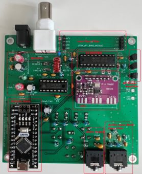
Building blocks of ADX Transceiver:
– Brain of ADX is an Arduino Nano which takes care of signal generation from audio tones of digital modes, user interface and calibration of SI5351 Module. ADX uses direct FSK Signal generating method similar to QDX or QRPGUYS Digital Transceiver III.
– Audio interface consists of a Speaker input from PC sound card which is actually an input to Arduino nano analog comparator for tone frequency detection and sampling. Before inputting signal to analog comparator of Arduino it passes through a band pass filter which has an audio band pass frequency range of 500 Hz to 3500 Hz.
This input acts like a VOX so no need for any PTT or serial PTT CAT input. When ADX hears a tone from for example WSJT/X audio output it starts transmitting. And when the tone of digital mode stops it stops TX. It’s that simple. The AFP-FSK (Audio frequency processed Frequency shift keying) technique used in ADX is developed by Burkhard Kainka(DK7JD) – http://elektronik-labor.de/HF/SDRtxFSK2.html
So how does this actually work?
Any digital tonal mode consists of varying audio tones that change frequency in relation to the data they correlate to. This audio tone generated for example for FT8 with WSJT/X software is passed through an audio band pass filter and then it is compared with Arduino Nano’s Atmega328P processor A/D comparator for start and stop zero cross detection to determine period of that tone. From that period, frequency of that particular tone that is determined and added to base transmit frequency, for example 14074000 Hz for 20m FT8. If the tone let’s say is 1000 Hz then the carrier TX is now 14074000 Hz + 1000 Hz = 14075000 Hz.
As it is summed it will be in USB frequency range of any SSB receiver though the signal is not pure SSB signal still any SSB TRX set to USB can’t tell the difference! This tone frequency detection and adding to base frequency is continuously repeated 400 times per second and refreshed until the FT8 tone transmission generation is over. In that case TX stops.
What fascinates me about this FSK signal generation technique is to generate a signal that is received in USB without any SSB mixing or filtering which eliminates problems of IMD or phase differences etc. that comes with SSB signal generation technique which allows such a simple Transceiver to be conceived with minimal parts.
– VFO: VFO is a classic cheap SI5351 Module from Aliexpress or any other site similar to that. VFO generates CLK0 TX signal, CLK1 RX signal and CLK2 calibration signal. No need to modify SI5351 Module as we did in uSDX rig builds. SI5351 module works in a cozy 400khz I2C speed.
– TX BUFFER: TX buffer is an inverting 74ACT244 octal buffer connected in parallel to drive Class E RF power amplifier consisting of 3 x BS170 mosfets. RF power output – varies from band to band – around 5 watts.
– Low Pass Filter Module is a serial resonance class E LPF filter similar to that one used in uSDX designs.
– RECEIVER is CD2003GP – A Chinese clone of Toshiba’s TA2003GP AM/FM radio IC. Only AM section is used as a direct conversion receiver.
– And some caps for RF and VCC filtering etc.
– 5 LEDs and three tactile pushbutton switches for user visual interface and controls. No fancy displays or rotary encoders!
– – Now we have CAT support! :)
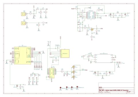
Here is ADX Schematics:
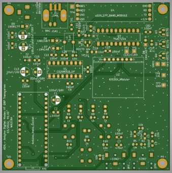
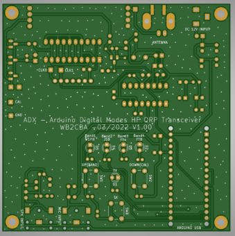
Here is ADX PCB layouts:
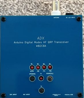
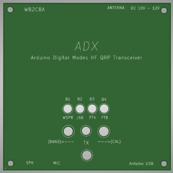
These are Top and Bottom Panels to give a professional rig appearance to ADX !
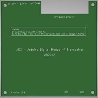
ADX Top Panel with LPF carrier slots:
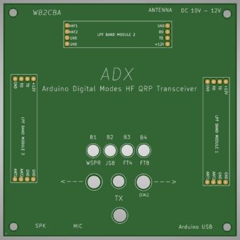
I even designed a top panel with LPF carrier slots so that extra 3 band LPFs can be carried on top of ADX transceiver! How crazy is that!
1- Building ADX:
Building ADX is simple and straight forward. All the files including Gerbers for PCBs and ADX firmware can be found in my GITHUB page on this link:
https://github.com/WB2CBA/ADX
Here is list of essential files in ADX Github page:
– ADX PCB gerber File
– ADX TOP panel Gerber File
– ADX BOTTOM panel Gerber File
– uSDX mOnO LPF Band Module Gerber File
– ADX Arduino Firmware
– SI5351 Library
– ADX User Build Guide – which is this write up
– ADX band dependent LPF Component Selection Excel sheet
– ADX BOM(Bill Of Materials) Excel Sheet
– The first step is to download all these files from ADX Github page.
– Now we need to order PCBs( Printed Circuit Board) for ADX :
The easiest way is to order from a Chinese PCB house online. I generally use www.jlcpcb.com . JLCPCB’s production is good quality , relatively cheap compared to quality and fast though shipping might be pricey if DHL is chosen to be faster. A cheaper shipping method is via snail mail which is regular post service though it is much slower.
To order a PCB first create an account with JLCPCB and upload supplied GERBER files in github page. There are videos on youtube how to upload and order PCBs from any of these online PCB houses. I strongly recommend to watch those if you haven’t ordered a pcb before.
– BOM excel sheet has all parts used in ADX. Parts used in ADX are not critical and not effected by part shortage as of writing of this article!
– Now if all parts and PCBs are gathered it is time to solder main pcb. I generally start with resistors and then capacitors. Then MOSFETS and LEDs and tactile switches. Don’t make an error, LEDs and switches are soldered on solder side of PCB!
– When soldering LEDs first solder switches. Then adjust LEDs so that top of each LED is flush with the top of switch lever. This way LEDs can stick their head nicely out of the top panel holes. Tactile Switches should be 6 mm lever ones.
– Now we can solder IC sockets and Arduino headers. I strongly recommend to use headers for Arduino nano. This way if something is not right it will be easy to replace nano. Same goes for IC’s.
– You can solder SI5351 module straight on to the pcb.
– The last items to solder are BNC, Power socket, Audio jack connectors and LPF headers.
– CX-1 is an optional capacitor for single band build giving a better band pass capacity. I added for experimental purposes. Not needed for the time being. Leave it blank.
– LX-1 is 1uH inductor made up of T37-2 toroid with 16 turns of 0.40 mm (AWG 26) enameled copper wire. (Also a fixed 1uH inductor can be used.)
This will complete main ADX PCB Build.
Now it is time to build LPF Band Filter Modules!
To use full four band capability of ADX Transceiver you need to choose four bands among 7 bands ADX supports.
These bands are 80m/3.5Mhz, 40m/7Mhz, 30m/10Mhz, 20m/14Mhz, 17m/18Mhz, 15m/21 Mhz and 10m/28Mhz.
Now for the chosen four bands four LPF band Modules needs to be assembled! By switching these 4 band LPF modules 4 different bands to operate can be covered.
2- ADX Band specific LPF(Low Pass Filter) BAND Modules:
ADX Transceiver uses Serial Resonance Low pass filter modules for each band it operates. For each band we choose to operate on we need to build a Band LPF Filter Module. We will swap these modules for the band we will operate on. Let’s say we want to operate FT8 on 40m/7Mhz band. Then we will grab and plug in 40m/7Mhz Band Module and select that band on ADX and Voila! Now we can operate ADX on 40m/7Mhz. Same applies to other bands. Although ADX is a mono band transceiver these plug in band modules gives it a multiband capability and flexibility.
ADX uses same LPF band module PCB of my uSDX mOnO transceiver. This way I didn’t have to design a new module. Lazy!
LPF band module PCB’s can be ordered by using GERBER file for uSDX mOnOLPF band Module.
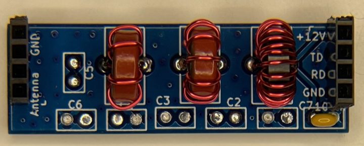
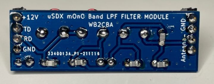
These Band filter modules can be built either using surface mount device (SMD)capacitors or through hole device(THD) capacitors.
Capacitor footprint on band module pcb allows to use 0805 or 1206 footprint standard SMD(Surface Mount Device) capacitors or 2.54 mm lead spacing THD(through hole) capacitors.
Toroids used are:
1x FT37-43
2 x T37-2 Red toroid or T37-6 Yellow toroid depending on band selection for each band module. Up to 20m/14Mhz band T37-2 toroids work pretty good. From 17m/18Mhz band to 15m/28Mhz band T37-6 yellow toroids are used.
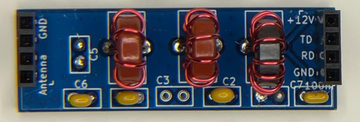
Here is a photo of Band filter module built using THD(Through hole Device) capacitors:
Photos of same filter built with SMD capacitors:
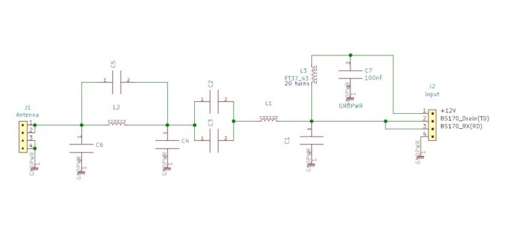
Schematic of Band LPF Module:
BOM for LPF Band Module:
2 x 4 pin header – These headers can be male or female headers depending on what is soldered on RF board. These band module headers should the opposite mate of RF board 4 pin headers. i.e if we used male 4 pin headers on RF board then Band modules must have female 4 pin headers to plug in and vice versa.
1 x C1 – Band Dependent THD or 0805 NPO 100V or more Capacitor
1 x C2 – Band Dependent THD or 0805 NPO 100V or more Capacitor
1 x C3 – Band Dependent THD or 0805 NPO 100V or more Capacitor
1 x C4 – Band Dependent THD or 0805 NPO 100V or more Capacitor
1 x C5 – Band Dependent THD or 0805 NPO 100V or more Capacitor
1 x C6 – Band Dependent THD or 0805 NPO 100V or more Capacitor
1 x C7 – 100 nF THD or 0805 Capacitor (Non band dependent capacitor)
1 x L1 – T37-2 RED or T37-6 YELLOW toroid – Band dependent
1 x L2 – T37-2 RED or T37-6 YELLOW toroid – Band dependent
1 x L3 – FT37-43 Ferrite Toroid – 20 turns. Non band dependent and same detail applies to all band LPF Modules.
AWG 26 or 0.40 mm enameled copper wire can be used for Toroid turns.
So how are we going to know which capacitor values for each band required and what Toroid to be used for L1, L2 and L3 and turn for each band?
This table will help us choosing all band dependent component values and details for each band. Beware that these values are a bit differing from uSDX mOnO band module values, they are optimized for ADX Transceiver.
This table is a base for building various band LPF modules. If you have a knack to experiment and need a bit more power here are some useful tips:
1- Lower one turn from L1 in each band. This will slightly increase RF output power though might increase TX current too so exercise caution!
2- For L3 12 turns also works pretty good so this can be a nice option to play with.
Though caution here! DO NOT EXCEED 5 WATTS RF POWER! Otherwise BS170 voltage limit will be exceeded which will end up in magic smoke!
CLASS E RF POWER AMPLIFIER BASICS and Some useful tinkering knowledge:
ADX Transceiver uses Class E type RF power amplifier scheme. Class E is an efficient class of power amplifier which can go up to 85 to 90 % efficiency which means less thermal heat dissipation on RF power transistors and lower supply current vs more RF power output. These are the advantages of Class E RF amplifiers. Disadvantage of this amplifier type is it is harder to tune and get the required efficiency when compared to other classes like Class A,B or C amplifiers. ADX uses this efficient class E amplifier like uSDX transceiver. 3 x BS170 mosfet transistors parallel when tuned properly can easily give up to 5 watts RF output power without dissipating any excess heat under 12V DC.
uSDX mOnO LPF band filter board consists of all parts related to fine tune ADX Class E mosfet Power amplifier. Above table has component values of each LPF Band Filter which will give a reasonable power efficiency on all 6 bands covered. Efficiency values for each band can be further tweaked and it is a great way to learn and experiment with class E amplifiers. ADX uses so called serial resonance LPF design for Class E and all values are calculated by WA0ITP’s excellent excel Class E design spreadsheet: http://www.wa0itp.com/class%20e%20design.html
Here are some class E readouts for curious ADX kit Builders:
http://www.norcalqrp.org/files/Class_E_Amplifiers.pdf
https://people.physics.anu.edu.au/~dxt103/class-e
TIPS on TOROID Winding:
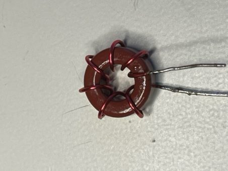
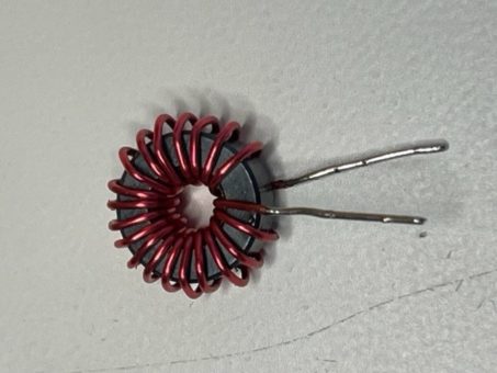
This is T37-2 RED Toroid with 7 turns of enameled copper wire.
This is FT37-43 L3 Toroid with 20 turns of enameled copper wire.
One important point to consider is that the edges of FT37-43 Toroids are quite sharp which can scrape enamel coating on inductor wire. To fix this issue the easiest method is tapering the edge a little with an oversized drill bit. Use the oversized drill bit to turn with your fingers inside the toroid ring to smoothen out sharp edges. Do not use a drill to turn the drill bit! You will snap the toroid and most importantly will harm your fingers in the process!
3- One turn means enameled copper wire passes once inside the toroid ring. For example, in 7 turns T37-2 toroid in the above photo wire passes 7 times inside the ring.
4- Always after passing the turn stretch the wire so it is tightly wound around the toroid.
5- When all turns are in count carefully every turn that passes through the inner ring of toroid. The best method to do is to take a close up photo of the toroid and count the turns. This way it is easier to see turns and you won’t miss a turn.
6- Never ever let one turn go over another one. Every turn should be side by side! This is important in toroids that have 20 or more turns and it is easy to overlap turns.
7- Always scrape ends of toroids to clean enamel coating for soldering. To clean enamel coating there are two methods which can be used separately or together.
Scraping enamel coating with a cutter knife thoroughly and then apply a bit solder coating. Second method is to heat up wire with soldering iron so that enamel coating just burns out and then cover with a solder coating. Scraping first and then burning the residue enamel coating is the best approach! Then apply a bit solder coating before soldering toroid into pcb.
8- Before soldering wound toroid try to spread as even as possible as in the photos above.
9- After soldering toroid in its place check with a continuity tester if solder joints are okay and connected electrically.
ADX CLASS E RF POWER AMPLIFIER MOSFET HIGH SWR PROTECTION and SI5351 Pull Up resistors Fix:
While experimenting with ADX transceiver I smoked out BS170 mosfet many times due to high SWR or operating without antenna! :)
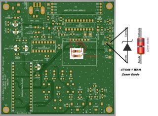
So I tinkered to find a way to prevent MOSFET demise in case of bad or excessive SWR! And thankfully we have a very simple solution for solution to prevent just that! :) A 47Volt 1 Watt zener diode is all needed and works like charm! The beauty of this zener protection is even without antenna no harm will be done to PA Mosfets!
Solder 47V / 1 Watt zener diode as shown in the photo above between TP3 and GND solder points in ADX PCB. Cathode of Zener Diode goes to TP3 test point and Anode of zener diode goes to GND1 test point. Zener diode can be any zener diode with 47V and 1 Watt rating. I used 1N4756 from On semiconductor. The other option can be BZX85C47 zener.
This will protect your PA mosfets from accidental smoke out! I strongly recommend to add this zener to your ADX pcb.
Here is my test video on youtube with another variant of ADX called ADX UnO which identical to ADX but with smd components:
SI5351 Modules are coming in various qualities and they are not identical sadly. Some of these modules don’t have I2C pull up resistors on them. If there is no pull up resistor then Arduino can’t address I2C ports SDA and SCL as they are open collector and needs to be pulled up by 10k resistors. If you are experiencing SI5351 related no signal generation fault it will be a good idea to add those two 10k resistors as shown in the photo above to cure that problem.
ADX FIRMWARE:
ADX firmware is developed in Arduino C language and Arduino IDE can be used for visualization and experimenting with it.
ADX uses Arduino Nano board as microcontroller. This is a readily available and cheap Arduino development board that can be outsourced easily online.
The current version is updated to ADX CAT VX.X. X.X stands for version number. This will change as new features will be added. I will continue working on firmware in the future so this version number can increase with new features. So check out occasionally ADX Github site for an update! New features are listed at the first page of this manual in bold.
SI5351 needs an Arduino library to work with. This library is Jason Mildrum, NT7S’s SI5351 library, Si5351Arduino-master.zip .
DO NOT USE Jason Mildrum NT7S’s latest version of SI5351 library from his github site as it is not compatible anymore with ADX firmware. Use SI5351 Library that is in ADX Github firmware page to avoid any I2C communication problems. ADX is using version 2.1.3 of NT7S SI5351 Library.
Install this library as you install any Arduino library. Using Sketch/Include Library/Add .ZIP Library menu. Just select the above .zip file and it installs. Do not unzip the file!
ADX_CAT_VX.X.ino is the ADX firmware file and can be downloaded from ADX github page:
Before we upload ADX firmware we need to setup band assignment in the firmware for our needs! Which is assigning four preferred bands we plan to operate on:
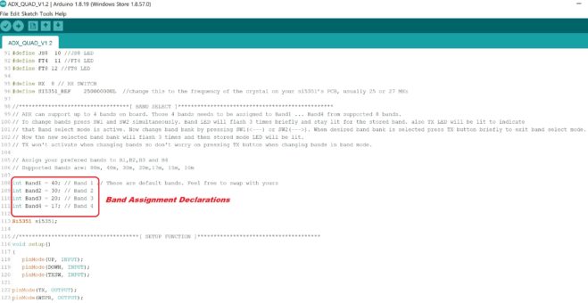
This is the band assign code lines from ADX firmware which needs to tailored for our preference:
Assign your own preferred bands to those locations in the firmware which is inside the red rectangle above. My preferred bands are 40m for Band1, 30m for Band2, 20m for Band3 and 17m for Band4.
After this band assignment we can compile and upload ADX firmware to Arduino Nano as uploading to any Arduino board. Nothing special here.
First Power up and smoke test!
After firmware upload we are ready for first smoke test! Do not install LPF Band module at this time. Connect 12V DC power source.
DO NOT USE More than 12V DC for ADX Transceiver as this pushes RF power output beyond 5 Watts and over 60V which is over max limit of BS170 MOSFETS. This can release magic smoke on mosfets!
Now measure voltage of 12V and 5V in different locations such as IC VCC pins etc. to make sure everyone gets the right voltage share!
If all is ok in terms of voltage now we can test if SI5351 is generating any signal. To do this use a frequency counter or oscilloscope on CLK1 test point. The default band is Band 1 and default mode is FT8. You should observe your choice of band 1 base frequency for FT8. For example in my case my Band1 is 40m and for FT8 it is 7074000 Hz or anything close to that as we didn’t yet calibrated the SI5351 VFO. The important point is to see some kind of signal generation which is tell tale of SI5351 is working!
If no smoke and nasty smell and there is signal from SI5351 then we are in business and passed smoke test!
Calibration Procedure for SI5351 VFO: (Updated in Version 1.1 firmware)
For SI5351 VFO Calibration Procedure follow these steps:
Calibration Procedure for SI5351 VFO: (Updated in Version 1.1 firmware)
For SI5351 VFO Calibration Procedure follow these steps:
1 – Connect CAL test point and GND test point on ADX PCB to a Frequency Counter or Oscilloscope that can measure 1 Mhz up to 1Hz accurately.
2 – Press SW2 / —>(CAL) pushbutton and hold.
4- Power up with 12V or with 5V by using Arduino Nano USB socket while still pressing SW2 / —>(CAL) pushbutton.
5 – When FT8 LED and WSPR LED flashes 3 times and stay on, release SW2 / —>(CAL).
Now Calibration mode is active.
6 – Using SW1(<—) and SW2(—>) pushbuttons change the Calibration frequency until reading 1 Mhz = 1000000 Hz exact to the nearest hertz on Frequency counter or Oscilloscope.
The waveform is Square wave so frequency calculation can be performed easily.
7 – If you read as accurate as possible 1000000 Hz then calibration is done.
8 – Now we must save calibration value to EEPROM location.
9 – In order to save calibration value press TX button briefly. TX LED will flash 3 times which indicates that Calibration value is saved.
10 – Now Power off ADX.
DO NOT FORGET TO SAVE CALIBRATION VALUE BY PRESSING TX BUTTON BRIEFLY AT THE END OF EACH CALIBRATION SESSION. OTHERWISE CALIBRATION WILL REVERT TO THE DEFAULT VALUE.
Calibration value is stored in EEPROM of Arduino Nano and will be loaded back in every power up so no need to repeat calibration once done. Also new firmware update won’t reset calibration and no need to re-calibrate again.
After calibration, plug in desired LPF band module. To activate Transmit for testing purposes we can always use TX button which acts as a ordinary PTT(Push To Talk) button and no need to connect to a digital modes software for transmit. This RF outputs a continuous wave signal only for testing RF power. Also this can be used for Antenna Tuner tuning.
Using ADX Arduino Digital Modes Transceiver:
ADX Arduino Digital Modes Transceiver can be used with CAT control via USB or using Manual control via switches and LEDs.
1- Manual Control of ADX using keys and LEDs:
Operating Controls and switching bands:
1- When you power on ADX one of the LED’s will briefly flash 3 times and then another LED will be on solid. The first LED which was flashing 3 times indicates the active or selected BAND bank. By default it is Band1.
For example if the LED was blinking in BAND1 which is 40m band in my ADX now I know my ADX is set for operate on 40m band.
The second LED which is solid is showing the active MODE. For example if it is in FT8 then ADX will operate on 40m in FT8.
So how we will change band?
– Press < — and — > switches simultaneously briefly.
– One of the BAND LED will blink 3 times and stay solid. Also TX LED will be on. This doesn’t mean that we are transmitting anything! It is just an indicator to show we are in band switch mode.
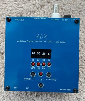
– Now using < — and — > switches we can turn on LED on different band banks. Of course we need to know which band is assigned to which bank. For that I use labeling tape to label each band bank corresponding to each band setup in the firmware.
See below photo for my band bank labeling as an example!
– After we select the band we would like to operate on, we can exit Band select mode by briefly pressing TX switch. As soon as we press TX switch the TX LED will turn off and the selected band’s LED will flash 3 times to notify us that is the band ADX will operate on. After blinking Band LED turns off, the mode LED will light up showing the mode we are on.
– Now we can scroll between modes with < — and — > switches. The on LED is the active mode. We can’t change band by scrolling left or right. This only changes operation mode such as FT8,FT4,JS8 or WSPR. To change band we need to simultaneously press two switches briefly. Then we enter band change mode which is indicated by TX LED on.
– Now the most important thing is not to smoke any finals! When we change a band we need to make sure that band’s LPF band module is plugged on!!!
Connecting ADX Transceiver to Computer and firing up ADX:
1- Connecting ADX Transceiver to any computer is pretty straight forward. We need a MIC which is Microphone input and SPK which is Speaker input or headphone input. We can either use PC built in soundcard or one of those cheap USB Soundcard adapters. I suggest to use a USB soundcard adapter for couple of reasons! This way if anything goes wrong built in soundcard won’t be damaged. Also this will help on ground loop instances.
For USB isolation and peace of mind from ground loop dangers you can use one of these before USB soundcard plug in:
https://www.amazon.com/GeeekPi-Isolator-ADUM3160-Isolation-Protection/dp/B07QKYYCD8/ref=asc_df_B07QKYYCD8/?tag=hyprod-20&linkCode=df0&hvadid=366402536789&hvpos=&hvnetw=g&hvrand=10336854439692763421&hvpone=&hvptwo=&hvqmt=&hvdev=c&hvdvcmdl=&hvlocint=&hvlocphy=9003562&hvtargid=pla-814018215075&psc=1&tag=&ref=&adgrpid=75347436439&hvpone=&hvptwo=&hvadid=366402536789&hvpos=&hvnetw=g&hvrand=10336854439692763421&hvqmt=&hvdev=c&hvdvcmdl=&hvlocint=&hvlocphy=9003562&hvtargid=pla-814018215075
For USB soundcard adapter I use this sound card from amazon:
https://www.amazon.com/Sabrent-External-Adapter-Windows-AU-MMSA/dp/B00IRVQ0F8/ref=asc_df_B00IRVQ0F8/?tag=hyprod-20&linkCode=df0&hvadid=312824707815&hvpos=&hvnetw=g&hvrand=7034552265858110987&hvpone=&hvptwo=&hvqmt=&hvdev=c&hvdvcmdl=&hvlocint=&hvlocphy=9004160&hvtargid=pla-563309581845&psc=1
– We also need 3.5mm audio jack male to 3,5 mm audio jack male extension adapter cables. Actually two of them!
Again from amazon I use this:
https://www.amazon.com/Syncwire-Braided-Auxiliary-Adapter-Headphones/dp/B01I0SI1SG/ref=sr_1_10?crid=33ELZO9OEPEH2&keywords=5mm+audio+cable&qid=1649788399&s=electronics&sprefix=5mm+audio+ca%2Celectronics%2C994&sr=1-10
These are just examples. You can get anything similar to these.
2- Connect Soundcard MIC input to ADX MIC input with one of the 3.5mm audio cables. To do the same connection from soundcard SPK output to ADX SPK input with the other 3.5mm audio cable.
3- Run WSJT/X or JSCALL software.
4- Power on ADX.
5- When you power on ADX one of the LED’s will briefly flash 3 times and then another LED will be on solid. The first LED which was flashing 3 times indicated the active selected BAND bank. So now we know which band we are going to operate on so double check if that LPF Band Module is plugged in and we are good to go! Enjoy ADX with Digital modes similar to any other HF Transceiver you will operate digital modes on!
For setting WSJT/X to work with ADX in Manual Mode:
– Go to Settings/Radio and activate PTT as VOX.
– Choose your soundcard under Settings/Audio menu
– Set Speaker Volume to 100%.
That’s all you need to start working with WSJT/X. This applies pretty much to other software such as JS8Call or WSJT/Z etc.
2- Using ADX in CAT control Mode:
ADX can be controlled with CAT – Computer Aided Transceiver – control too.
In CAT control mode ADX emulates KENWOOD TS2000 Transceiver CAT commands.
In CAT control, Frequency and TX/RX of ADX is controlled via CAT commands.
For example in WSJT/X CAT control can change bands, modes and control TX.
To operate on CAT:
– Connect Arduino Nano USB connection to PC USB port.
– Connect Audio jacks to MIC and Speaker of PC and ADX as in Manual mode described above.
Setup Audio in GUI application for your sound card. For example for WSJT/X, go to settings/audio menu and choose audio in and audio out sound card.
For CAT control SETUP:
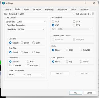
1- Choose KENWOOD TS2000 as transceiver
2- Choose comm port for your ADX com port from the com port list of your GUI software and set for 9600 bps, 8 data bits and 1 stop bit.
Here is WSJT/X CAT RADIO setup page for ADX as an example:
If all setup is selected right and USB is connected to ADX when Test CAT is pressed after a short pause it should be green. If it is green then CAT is working properly and active.
IMPORTANT POINTS WHEN OPERATING with CAT:
– When operating with CAT any band can be selected without any limitation though the important point is to plug in the right LPF Band filter module on ADX before band change!
If a wrong LPF filter is used for a band that is not matching the selected band with CAT this can damage BS170 PA mosfets.
– When CAT is active JS8CALL and FT4 LEDS will illuminate and none of those switches or leds will work. Only TX led will be working when TX is on. This manual control lock out is designed on purpose to prevent any conflicting commands between manual mode and CAT.
– CAT Test PTT check button on CAT setup won’t work as ADX does not have a physical PTT control via a pin or button and this is totally normal. ADX PTT is controlled via audio that is transmitted from GUI application like WSJT/X. CAT PTT selection setup can be CAT or VOX and won’t make much difference.
– When ADX is first powered up it starts in Manual control mode with switches and leds as usual. When CAT is activated it automatically enters into CAT mode with default 20m FT8 selected. Make sure to choose the right band and mode before starting TX in accordance with plugged in LPF Band Module.
– When ADX is in CAT mode it will be working only in CAT mode. To exit CAT mode recycle power by brief on/off. Now ADX will start in Manual control mode again.
ADX Limitations and areas that need improvement with wish list! And what is this rig’s purpose in life?
ADX is a simple transceiver that can operate only in digital modes and especially those four popular digital modes, FT8, FT4, JS8Call and WSPR with pin point frequency settings. These are slow tonal modes which Arduino can cope with capturing, decoding and generating FSK signal. Can this rig work on faster digital modes? May be. I am not sure. I haven’t tried but it won’t hurt to experiment with.
The firmware of ADX is basic and there is a lot of room to improve and speed up things. My Arduino programming capabilities are limited as you will witness from the code I put together :)
Receiver works with reasonable performance for such a simple and dirt cheap receiver design though this is another block that can benefit from improvements. A better band pass filter, an rf amplifier may be a good addition. Currently I am using LPF filter’s first stage band pass which is working pretty good! It’s a cheat! A QSD type RX stage like uSDX’s FST3253 will improve RX sensitivity and most important, selectivity.
An onboard soundcard with a USB onboard hub for Arduino serial might be a nice addition too for single point usb connection control with CAT!
A quad band LPF board with I2C band switching similar to my design uSDX QuadBand LPF board might be another addition which can automate things with a CAT interface!
The wish list goes on and on but it boils down to the same conclusion! I started to tinker with this rig to be a simple and dirt cheap HF transceiver which performs reasonable with minimal hardware to lure young Amateur Radio enthusiasts with a Geek mindset and DIY knack to Amateur Radio and digital modes. I think ADX is hitting all these bullet points as a beginner HF Transceiver. Any of these additions will blow the main purpose of existence of this simple HF digital modes transceiver. So I leave that evaluation to you…
My hope and wish is that this simple HF Transceiver to serve its purpose and attract young Hamradio beginers to Amateur Radio Hobby and DIY Amateur Radio community.
Acknowledgments:
I would like thank:
– Burkhard Kainka, DK7JD for his inspirational Audio FSK generation code for Arduino. Without it I would be still scratching my head how to solve this problem!
– Jason Mildrum, NT7S for his excellent SI5351 Arduino Library.
– ADX CAT code inspired from Lajos Höss, HA8HL TS2000 CAT implementation for Arduino.
– Improved FSK TX signal generation code of JE1RAV
– My friend Burcak Cubukcu, TA2EE for his building, testing and verifying all my ADX designs before releasing and his editorial skills on publishing ADX article and updates.
Last word: No usage restrictions or silly licenses on this design. This is a Free and Open Source design for the ham radio community. Feel free to use in any means including commercial usage. Sky is the limit!
Enjoy your Digital QSOs!
Barbaros Asuroglu aka Barb, WB2CBA
04/08/2023
wb2cba@gmail.com
An Alternative ADX Construction Manual
Thanks to Cowtown Amateur Radio Club you may download ADX Construction Manual here.

