uSDX – A Compact SOTA SSB SDR Transceiver with Arduino!
This is a write up to share my experiences of designing, building and testing of uSDX PCB V1.01.
The title sounds a bit surreal when SDR and Arduino are used in the same sentence! SDR so complex and micro computing hungry and Arduino Atmega328p so modest and simple when compared in power. That was my thought when I first came across this brilliant project of Guido, PE1NNZ while searching web.
Now a small dose of my history. Being a radio ham for over 30 years I was never involved in HF and until last year not one qso, sounds embarrassing. I was more of a digital and micro guy with vhf and uhf experience as a ham and amateur satellite communications was my RF interest. It all started last year when I was searching for a simple long distance communication protocol for pico balloons and I found WSPR and I was hooked and mesmerized how such a simple protocol can go so far! I devised and programmed my own wspr transmitter with esp8266 and wrote an article on it here. Then I discovered FT8, FT4 and etc. Genie was out of the bottle by now and HF and digital modes were my new hobby!
I decided to design and build my own SOTA (Summit On The Air) transceiver solely for digital modes. I started with building a digital modes simple HF receiver and it worked pretty good. You can read about this receiver in this article: https://antrak.org.tr/blog/projeler/poor-mans-hf-ssb-receiver/
Then came the search for an SSB transmitter. I avoided DSB ones as it occupies two side bands though it is simple to build. I was searching on Tayloe modulation technique of Dan Tayloe and SDR ways of SSB filtering and modulation just to avoid complex balance modulators, crystal filters and inductors. Being a micro controller and software enthusiast, RF and inductor based complex circuits are not my forte at all.
Then one day Eureka moment! I found Guido’s (PE1NNZ) brilliant mod for QRP LABS QCX CW transceiver as an SDR SSB!
https://github.com/threeme3/QCX-SSB
This is what I was looking for. The QCX kit and Guido’s brilliantly written genius firmware together seemed to me the ideal match for a portable SOTA transceiver. I ordered a QCX from QRP LABS and modified it to test Guido’s firmware and mod. Worked like a charm. I used it for almost a month for my tests and qso’s. Though something was odd and bothering me. When I modified the QCX kit I ended up with a handful of unused parts and a pcb almost empty with dysfunctional holes and IC spaces.
Then came march and living in NY in March 2020 was not the safest thing due to COVID-19 spread. I had to shelter home for almost 2.5 months like all fellow New Yorkers. This gave me a tremendous opportunity to work on a new project. I wanted to create a pcb solely dedicated to Guido’s incredible firmware and create a SDR SSB transceiver for SOTA with a battery pack etc. The list was going on and on…
What is QCX SSB?
QCX is an amazing CW kit you can build, designed by Hans Summers, GOUPL and manufactured by QRP LABS which is owned by Hans Summers. I admire QRP LABS kits. It uses an ATMEGA328 as it’s controller. You can find the details of QCX here:
QCX is for CW only. Guido, PE1NNZ with his brilliant firmware converted QCX into a full SSB/CW SDR transceiver. Most of the SSB filtering and dsp functions are done in atmega328p running an Arduino sketch which works at 20 mhz. All that SSB digital filtering and functions on a 8 bit low end micro controller such as Atmega328p is an incredible feat of software engineering.
All the details and firmware of QCX SSB can be found here:
https://github.com/threeme3/QCX-SSB
uSDX PCB Version 1.00:
First task in hand was to create a schematic that is refined with components needed for Guido’s firmware to function properly. I took to the web to contact Guido and fellow QCX SSB users to clarify the QCX SSB schematic. Guido as always was very kind and helpful directed me to the right schematic that I should use.
I also joined uSDX forum in IO Groups. A great place with a lot of knowledge on RF and SDR. And it is dedicated for QCX SSB firmware and applications which is called now uSDX.
I started to put together a technical guidelines list of my new pcb design:
- It should be through hole – so that every fellow ham can build it with a soldering iron. No need to special tools, no need for rework stations and be practical.
- It should consist of one pcb.
- The pcb should be flat, the controls and display on the same plane like QCX. I found QCX design practical and easy to operate as a SOTA rig.
- Should be multi band with switchable LPF filters.
- Should use SI5351 modules to avoid smd SI5351 chip soldering which is not easy at all!
- A battery backpack that will last at least couple of hours of qso.
I designed and put together uSDX V1.00 test pcb and built it.
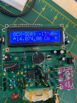
Here is uSDX V1.00:
As you will notice I had errors that had to be corrected with cutting knife and jumpers! But surprisingly it worked! I was amazed how well it worked. Here is the thread from UCX IO Groups with my experience on uSDX V1.00 pcb:
After testing the ver 1.00 pcb for sometime as a test bed I was convinced that it is a good candidate for my SOTA rig. I started to correct errors on pcb and uSDX V1.01 was born.
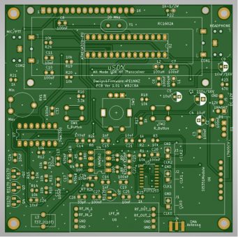
uSDX V1.01:
This is the pcb I aimed as my SOTA rig. It was corrected for errors on V1.00 and tested. It worked great and if you ignore the story part in this article this is all about V1.01 pcb and building it and trouble shooting. I will try to explain one by one.
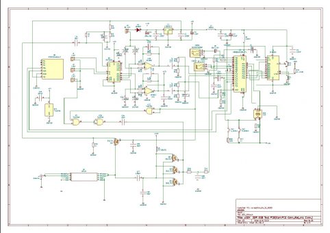
Here is the schematic of V1.01:
I will include all the design files and KiCAD files at the end of this article as zip files. Also the firmware modified to work with this pcb design will be in zip files.
Ordering the pcb:
Gerber Files are in uSDX_V1_01_06_06_2020.zip
You can use this file to order pcb of uSDX from any pcb manufacturer. I use www.pcbway.com in China. They have reasonably cheap prices and fast return time if you choose DHL or FEDEX for delivery. 10 pcb costs 5 US Dollars + shipment.
For ordering you choose default values. Just enter pcb size as 98mm x 98 mm and choose how many pcbs you need. Then you add your selection to cart and upload gerber file to them which is this zip file. You don’t need to extract zip file just upload as it is.
They will review your gerber for suitability for manufacturing and send you an email notifying you that your pcb is approved for manufacturing and waiting for your payment. You can pay with paypal.
Putting Together the uSDX V1.01:
Component Selection:
I used below listed pcb dependent components from these retailers:
Headphone and mic/PTT pcb type jacks are CUI SJ1-3523N
https://www.digikey.com/product-detail/en/cui-devices/SJ1-3523N/CP1-3523N-ND/738689
FST3253 is SOIC 16 type FST3253MX:
74ACT00 in DIP 14 PIN case:
https://www.digikey.com/product-detail/en/texas-instruments/SN74ACT00N/296-4348-5-ND/375717
SI5351 Module:
https://www.adafruit.com/product/2045
or if you search on any site like Aliexpress.com , ebay.com, amazon.com as SI5351 Module.
2×16 LCD Display:
It is a standard 2×16 display nothing special. The most important thing is pins should be on top of the display. Pin number 1 on the left and pin number 16 is the most far right one.
I got my display from amazon.com
Rotary Encoder:
You can use any rotary encoder from Aliexpress or ebay with switch version meaning it has to have a push button switch when you press encoder shaft. Generally, 5 pin ones are the switched ones.
I am quite happy with these BOURNS ones from Digikey. They are a bit expensive but worth the money.
https://www.digikey.com/product-detail/en/bourns-inc/PEC11L-4115F-S0020/PEC11L-4115F-S0020-ND/4699168
RV1 potentiometer:
It is a PIHER 10 mm type
Resistors:
For resistors I used ¼ watt %1 metal film ones. Especially for R10,R11,R12 and R13 voltage dividers. For R22 which is the backlight limiter for LCD it is good practice to use 1/2watt to allow heat dissipation if it happens.
Capacitors:
Pins with 2.50 mm spacing, the smallest ones you can find.
https://www.digikey.com/product-detail/en/kemet/C315C103M5U5TA7301/399-13973-1-ND/6562544
Similar to this in size will be a good fit.
LPF (Low Pass Filter):
I used LPF from QRP LABS. Here is the link:
https://www.qrp-labs.com/lpfkit.html
On a side note, there is no C29, C30, C31, C32 in the schematic. These were the capacitors for lpf filter in my very first version of pcb for single band then deleted them and used LPF filter module from QRP LABS.
I always use IC sockets for IC’s just in case of smoke it is easy to replace. For atmega328p definitely use a socket as you have to swap IC in firmware updates. A precision socket might be a good choice.
Jon, KE5URU kindly put together a BOM list which is below:
WB2CBA Board Building of Materials BOM
Modifying SI 5351 Module:
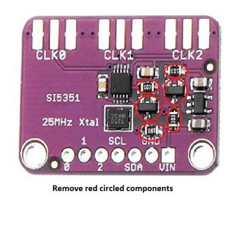
Step 1 is to desolder 6 components.
4 smd resistors and two smd level shift transistors. Shown as red circled ones below.
After de-soldering your SI5351 module should look like this:
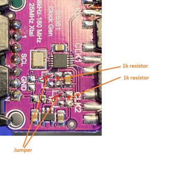
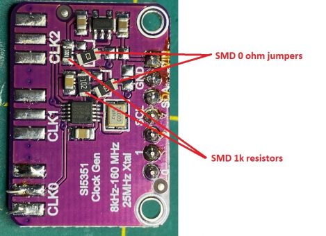
Step 2 is to solder two 1k smd resistors and two jumpers shown as below:
Use a rework station if you have or a fine tipped soldering iron for these modifications. You don’t necessarily have to use a 0 ohm resistor for jumpers. You can use a short wire also. It is neat to use 0 ohm smd resistors though. Also smd 1k resistors are not a must. 1k ¼ or 1/8 watt resistors can be used too.
SI5351 modification is done. Why we have to go through this? Guido’s QCX SSB firmware uses a fast I2C communication almost at the limit. The level shifter mosfets and 10k resistors as it had a hard time to cope with this speed in my tests and I found that it is much easier for SI5351 to work with this modification.
Soldering and Building:
FST3253:
This is the only smd IC on the pcb. It is relatively easy to solder with a clean fine tip iron. Solder this first on the pcb as it is easy when the pcb is not populated.
- I personally start with IC sockets, headphone jacks, headers for LCD and LPF, SMA jack and push button switches. Do not solder rotary encoder yet.
- Resistors come next
- Then Capacitors.
- BS170 transistors
- L3 T37/2 inductor
- Then 7805 and rotary encoder.
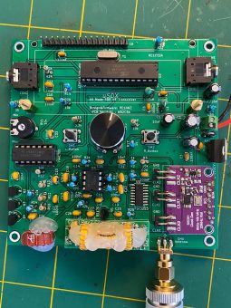
- Solder SI5351 module in it’s place. I soldered it straight without header but it is a preference. Header can be used too.
Of course this is not a must procedure list to follow and every fellow ham has their own way so follow your instincts and have fun ?
Programming ATMEGA328P (the easy way):
uSDX V1.01 pcb does not contain an ISP port. I thought I don’t need one as I am using this method which I will explain below.
- Buy an Arduino uno. Arduino uno is a cheap board which actually started the Arduino revolution. It uses atmega328p in DIP package. NOT THE SMD ONE!
Such as this one:
- In Step 2 connect it to your computer via USB and run Arduino IDE to program Arduino UNO with the uSDXV1_01_06182020.ino file from the zip files below this article.
- If the programming completed successfully remove the atmega328p chip from Arduino uno and plug into your uSDX pcb. You are done!
If there will be a new release from Guido then you can unplug atmega328p from uSDX and plug it to the Arduino uno board and upload the new firmware and swap again to uSDX.
————UPDATE v1————
uSDX V1.01 PCB Corrections and Improvement Modifications
After using sometime uSDX V1.01 pcb and in the light of the new discussions around FST3253 pin 1 left open and effecting adversely the reception quality I decided to put together this guide to modify and improve uSDX PCB V1.01 specs.
There are three modifications to carry out and they are pretty easy to do. I will walk you through all of them one by one .
1- The 10 nF Capacitor at Q1 BS170 Drain to LPF:
This is rather embarrassing on my part! I forgot it! I am sorry for this. Ok this capacitor decouples the BS170 isloation Mosfet drain from TX path and it has an effect on TX power. I noticed my error when working on uSDX V1.02 ☹
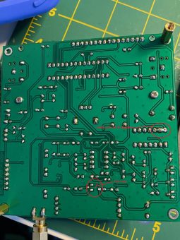
Here is the location of the track where we have to cut and insert the 10 nf capacitor:
In this photo the red circle which is designated as cut trace is where the 10 nf forgotten capacitor will be inserted.
The 74ACT00 pins12, 13 are floating gate pins which will be soldered to pin14 which is VCC for 74ACT00. I will explain this on item 2.
Cut the trace with an exacto cutter knife as shown below:
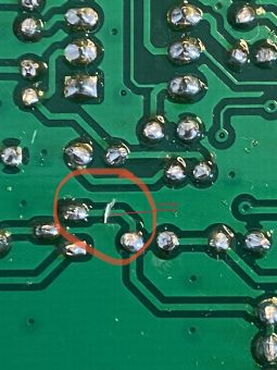
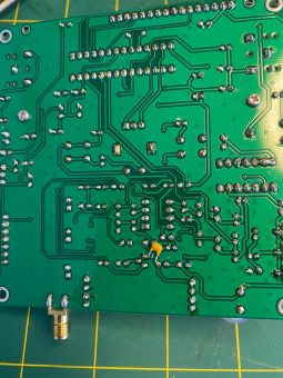
Then solder a 10 nF capacitor between BS170 Drain and C27/100nF pad as shown in the photo:
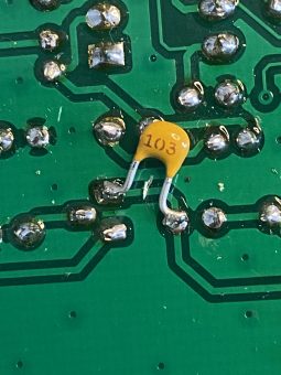
This will sort out the forgotten 10nF capacitor issue.
Here is a general view of the board showing the soldered capacitor.
2- 74ACT00 gate 4 input pins 12 and 13 floating:
It is always a good practice to tie in floating/unused input pins of CMOS logic to either VCC or ground and I didn’t do it. Another embarrassment on my part!
Here is how to sort this issue:
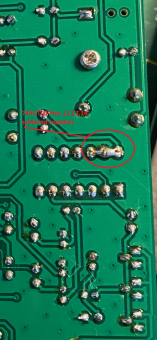
Simply solder pins 12 and 13 of 74ACT00 to pin 14 which is VCC(+5V) by shorting all three with solder blobs like in the photo above. This will take those floating unsued pins to logic 1 level and 74ACT00 will be a happy customer ?
3- FST3253 Pin 1 floating issue:
FST3253 Pin 1 is the first switch enable pin which is the unused switch. FST3253 datasheet logic table shows that if this pin is low or tied to Ground then switch 1 is active and if it is tied to VCC then inactive or disabled. When it is not tied to any logic level then the transients are effecting the RX overall performance and increased noise figure. Thanks to Scot Forshaw, 2E0WWV and his thread this improved a lot the reception noise figure.
Here is the thread discussing this issue and solution:
Here is the solution for FST3253 pin1:
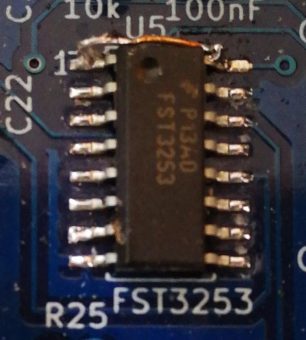
Just solder a short wire between pin 1 and pin16 of FST3253. Pin16 is VCC and this will pull pin1 to +5V logic level which disables switch 1.
I hope these mods and corrections and photos are clear. if you have any questions please send me an email
————UPDATE v1————
Fun Starts! Power up and first tests:
After soldering is complete and all parts are in it is always a good idea to double check for bad solder joints, misplaced parts and shorts. This prevents the nasty smell of smoking components on power up.
If you have a adjustable power supply for initial tests 12V/600 ma setting will be good. Power up and measure 5 volts and 12 volts first.
- Measure 5 volts on 74act00 pins 14 and 7. Pin 14 is +5v and pin 7 is ground.
- For 12 volt use LM4562 pins 8 and 4. Pin 8 is 12 volt and pin 4 is ground. At this point if there is no smoke we passed the first test.
- On receive the current consumption should be around 60 to 70 miliamps.
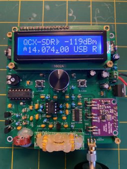
This should be the display you should get:
- If you see QCX_SDR then you are in the sdr mode. Unplug LCD and measure Aref pin voltage which is Pin 21 of Atmega chip. You should see around 1.1 volts.
- Now measure voltages on Atmega chip pin 23 and pin 24. You should get around 0.55 volts.
If these are the voltages you get then your rx should work if you connect an antenna.
- Testing TX:
- Use a wattmeter and a dummy load connected to antenna output sma connector.
- Choose CW with right pushbutton.
- Prepare a dummy PTT switch with a 3.5 mm jack and push button.
Mic connection of uSDX is:
MIC = TIP
RING = PTT
SLEEVE = GROUND
- Connect an amperemeter serial to power supply to measure current on transmit.
To adjust TX efficiency we will use two menus:
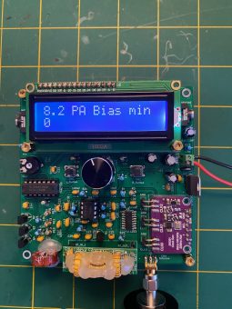
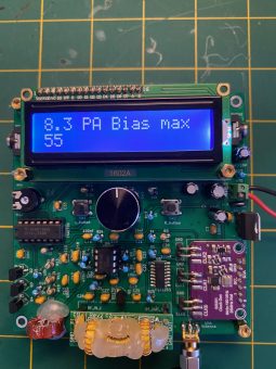
8.2 PA bias min and 8.3 PA bias max.
Ok this part is a bit tricky. You have to find a sweet spot by playing with these two values. The trick is to lower the amp drawn by TX while increasing the RF power output which is a game of efficiency. But don’t push to high output as BS170’s can heat up pretty quick. Especially in digital modes with long TX times BS170’s heat up and smoke. I changed 3 pairs! So watch out for the heat on them. What I found out is PA bias min= 0 worked for both of my prototypes V1.00 and V1.01. PA bias max for me is between 55 and 128. But it might be different for other builds depending on transistor characteristic differences and other component tolerances. The TX current under 12 volts for me was between 400 miliamps and 520 miliamps. Above that BS170’s heat up pretty fast.
RF power of 3.0 to 3.5 watts was safe for my transceiver. Pushing beyond that was heating up BS170’s in digital modes.
Now uSDX is ready for a run. Connect to an antenna and give it a go.
Troubleshooting:
QCX DSP on start up screen:
This was my first trouble when I built the V1.00. Guido advised me to check Aref and ADC1 and 2 voltages. Check voltages on Aref which is pin 21 of Atmega328p to see if it is 1.1V. Also check the ADC1 and ADC2 pins which are pin 23 and pin 24 of Atmega. They should be around 0.55V.
If these voltages are more than what I listed then check your R10, R11, R12 and R13 values. uSDX enters this mode when there is a difference between ADC1 and ADC2.
This is how Guido explained me the QCX DSP mode:
“ At line 2702 the qcx tries to detect if the ADC1 and ADC2 inputs are about the same voltage, if so it concludes that there is an SDR receiver. So probably there are some resistor differences in the adc bias network that are causing the radio to start in dsp mode… Check bias differences as it might also impact the RX side-band rejection.”
It can be forced into QCX-SDR mode by removing the slashes of line 2718: //ssb_cap = 1; dsp_cap = 2; // force SSB and SDR capability
This issue was my major problem. I can’t think of any other major issue. it worked pretty good.
Adjusting TX power was fun with trial and error and smoking couple of BS170’s in the process.
Here is my ucx iogroups thread once more about my uSDX V1.00 experience and troubleshooting for your reference.
Some helpful hints about uSDX PCB V1.01 build:
- Adjusting SI5351 25 mhz crystal value in the firmware:
- If you use uSDX_V1_01_06062020.ino from the zip file below then it is already modified for this pcb with SI5351 module.
If you download QCXSSB.ino from Guido’s github then you have to modify it for 25 mhz SI 5351 xtal value.
Comment line 896
Uncomment line 897
Line 896 //#define F_XTAL 27005000 // Crystal freq in Hz, nominal frequency 27004300
Line 897 #define F_XTAL 25004000 // Alternate SI clock
It should look like this.
Mic and Headphone Connections:
MIC 3.5 mm Jack connection is as follows:
TIP = MIC input
RING = PTT
SLEEVE = Ground
Headphone 3.5mm Jack Connection is as follows:
TIP = Audio out
RING = Audio out
SLEEVE = Ground
Audio Line out vs Speaker:
Resistor R23/470 ohm inserted between C9/10uf and PB1/Pin15 of Atmega328P as a limiter and adjusts the output level suitable for soundcards, active speakers etc.
If R23 is shorted a conventional speaker can be connected and PB1/Pin15 audio out will be able to drive it.
Changing Rotation direction of Rotary Encoder:
If Rotation direction of the rotary encoder is not right it is very easy to change it:
Line 16 #define ROT_A 6 //PD6 (pin 12)
Line 17 #define ROT_B 7 //PD7 (pin 13)
In the firmware swap 6 and 7 pin numbers in line 16 and line 17.
Forcing uSDX to QCX SDR Mode from QCX DSP:
To force firmware to start in QCX SDR mode:
Uncomment line 2718
2718: //ssb_cap = 1; dsp_cap = 2; // force SSB and SDR capability
Uncomment means removing the slashes in the beginning of a line
Comment means adding slashes to the beginning of a line.
L3 and C28 Band dependent L/C pair:
These two components are the most crucial components for the RF power amplifier. There is a whole discussion about these in UCX forum.
I conducted my tests on 20m/14 mhz band. For 20 m C28 = 33 pf and L3 which is T37/2 is 10 turn winding which brings it around 0.45 uH.
For other bands a good reference is QCX manual which is linked below. The values for different bands can be picked up from this manual. I believe in QCX it is L4/C30 combination which corresponds to L3/C28 in uSDX pcb.
https://www.qrp-labs.com/images/qcx/assembly_A4-Rev-5e.pdf
What’s next?
A smd version may be or just enjoy the summer and summit with the SOTA rig uSDX as it is with a beer! ?
I am working on a strap on battery backpack that goes under the pcb. Still testing. When all goes well I will write a post about building it with all the associated design files added.
A 3D printed case is desperately needed! That is beyond my abilities unfortunately. If a fellow ham designs a 3D case and shares the STL files that will be a home run to finish this project!
Conclusion:
This write up was aimed to help and share my experiences in designing building and testing of uSDX pcb v1.00 and ver 1.01 as a guide for fellow hams who wish to give it a go. I can assure you that you will have great fun with it.
This was by far the most fun project which kept me busy in these uncertain times with COVID-19 and I enjoyed it a lot.
I would like to thank Guido PE1NNZ for his great work and brilliant software skills. I still can’t wrap my head around how the heck he squeezed all those functions in a humble atmega328p. My respect to you Sir!
Files:
GERBER File:
uSDX Firmware:
uSDX_V1.02i hotfix applied firmwares for WB2CBA PCB V1.01 and V1.02
KICAD FILES:
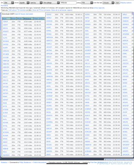
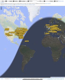
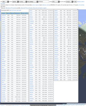
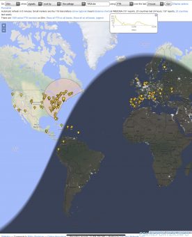
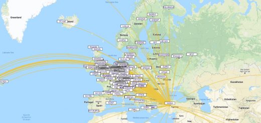
My FT8 RX and TX data from pskreporter.info with uSDX V1.01 pcb. Operating from my car with my 20 m whip antenna
Barbaros Asuroglu aka Barb
WB2CBA
NY 06/20/2020
wb2cba @ gmail.com
– This pcb design can not be used commercially without the consent of Barbaros Asuroglu WB2CBA.

