uSDX SOTA – Modular All Mode SDR HF Transceiver for QRP Operations
uSDX SOTA is not one design for one rig, it is more of a modular design to cover multiple configurations and options. It is also mostly SMD version to be able to kit it as in semi kit form. It is kind of Lego building blocks, modules of uSDX Transceiver.
I guess you all know by now my passion for designing my own compact SOTA rig. So this final design of uSDX Transceiver is named out of that passion as uSDX SOTA.
uSDX SOTA is a hamburger rig more like a BigMac, unlike DL2MAN, Manuel Klaerig’s elegant and neat sandwich design! :)
It’s a modular design with different stackable boards to create a flexible configuration transceiver for all needs.
Here are basic building blocks of uSDX SOTA System:
Main Board:
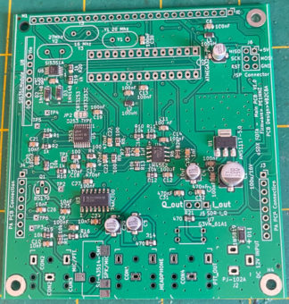
This main board is similar to my TriBand design main board. Has all components on board except PA+LPF parts. It has full CAT compatibility with USB interface also supports usb programming.
Power Amplifier/Low Pass Filter (PA/LPF) Boards:
For this we have 3 options or modules to choose from:
Quadband SMD Version
This is same as quadband THD version for 4 bands relays and all parts except PA Final BS170 Mosfets and Band LPF parts are surface mount device(smd).
Quadband THD Version PA/LPF Module:
It is released in this link:
https://antrak.org.tr/blog/quadband-4-band-palpf-board-for-usdx-triband-an-all-mode-hf-qrp-transceiver/
Octoband THD version PA/LPF Module:
https://antrak.org.tr/blog/projeler/octoband-usdx/
All these PA+LPF Modules can work with uSDX SOTA Main Board and they are fully compatible.
Display Boards:
There are two types of display boards to choose from depending on which configuration of uSDX SOTA rig is chosen, with or without internal Automatic Antenna Tuner.
128×64 OLED Display Module:
This display board is used for uSDX SOTA Transceiver without internal automatic antenna tuner unit.
Dual 128×32 OLED display module with ATU Controls:
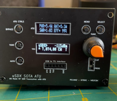
This display board is used to build uSDX SOTA ATU transceiver with built in automatic antenna tuner unit. We have two OLED displays, bottom one for uSDX transceiver operation display and top one is for automatic antenna tuner operation which displays RF power in, RF power out, SWR and efficiency percentage similar to an ATU 100 antenna tuner.
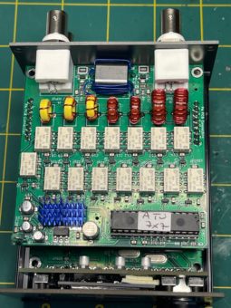
7X7 Automatic Antenna Tuner Unit (ATU) Module:
This ATU module is a shameless copy of David Fainitski, N7DDC’s infamous 7X7 ATU100 Antenna Tuner which is redesigned to be miniature enough to fit in uSDX SOTA aluminum case and work in QRP conditions up to 10 watts tested.
We can build two different type of uSDX SOTA Transceivers using these modules:
1 – USDX SOTA:
This version is uSDX SOTA Transceiver with similar appearance to uSDX TriBand using the same clamshell aluminum extruded case. No internal ATU, just a HF transceiver with chosen PA+LPF module.
uSDX SOTA configuration uses
– Main Board
– 128 x 64 OLED Display Board
– Any of the PA+LPF Boards outlined above.(QuadBand THT, QuadBand Smd, OCTOBAND THD)
– Fits into the same aluminum extruded clamshell enclosure as uSDX TriBand design.
uSDX SOTA ATU:
This is uSDX SOTA Transceiver with built in 7X7 ATU – Automatic Antenna Tuner Unit
This configuration Uses
– Main Board
– Dual 128 x 32 OLED ATU Controls Display Board
– Any of the PA+LPF Boards outlined above.
– 7X7 ATU Module
This configuration also uses same aluminum extruded enclosure with a small trick to fit all which I will explain in detail later in the blog.
So why so many modules and designs? What’s the story? I get that question a lot. The simple answer is evolution of design and learning curve on the way. I design one module and then evolve to another one etc.
For example in Triband design, 3 band slide switch was simple enough for me at that time for switching between bands and worked great though not fool proof so I jumped into Octoband 8 band module for relay switching.
It turned out to be a good option but overkill for this rig. 4 bands turned out to be more than enough for practical use on a portable SOTA/POTA rig so I designed Quadband pa+lpf board.
Then I had the crazy idea of designing all in SMD and get them manufactured. I never tried that before so that was another learning curve and adventure which I enjoyed a lot. Especially the idea of soldering less components per board!
There were a lot of discussion about ATU and if it is worth to include in this rig in my circle. To me it is worth to include. Why? Because I don’t have a stationary ham station and a fix good SWR antenna at home. Having an ATU to cover all antenna conditions is priceless to me. Is it lossy? Yes a bit. So what? Who cares? It is better than smoking my finals and peace of mind! Also in SOTA conditions when we are backpacking If we use a random end fed wire antenna then an ATU makes a lot of sense.
This design looks similar to uSDX TriBand so what is different or better? Let’s discuss that a bit.
uSDX TriBand was a satisfactory design for my needs though it was lacking two important functions:
– USB CAT interface
– USB Firmware Programming
CAT becomes a viable feature with relay switched band PA+LPF modules when using digital modes. It is always good to switch automatically bands on WSJT/X or any other CAT supporting PC software.
Programming of latest uSDX firmware into ATmega328p was a very annoying issue on my previous uSDX designs. In order to program the latest firmware you need to open the case and use ISP connectors or pry off the ATMEGA processor and program it then plug it back in is pain in the back!
In uSDX SOTA we don’t have to do that anymore. We just use that 6 pin female header in the display modules to program or for CAT. I will explain in detail these functions.
Also being able to use Octoband, 8 band PA+LPF or QuadBand 4 Band PA+LPF with or without an internal ATU brings a more flexible option on the table than TriBand design.
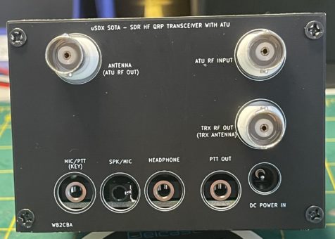
The rest of the specs and functions are almost identical to TriBand, SDR I/Q pins for experimenting with SDR output, PTT OUT for driving an amplifier directly with an optocouplee solid state relay TX, SPK/MIC for handheld speaker/Microphone, Headphone and MIC/PTT/Morse KEY inputs are all same features as in TriBand design. Also the aluminum enclosure is the same one that was used in TriBand.
Why I tried to keep uSDX SOTA as much as compatible with TriBand? I am sure out there are many fellow hams who have invested on TriBand boards and PA+LPF boards such as OCTOBAND or QUADBAND and would like to upgrade to uSDX SOTA. So this makes life easier for them to use their existing PA+LPF units or aluminum cases with these new transceiver modules.
There is one caviat though we can’t use anymore those slide switch PA+LPF modules with this new uSDX SOTA Mainboard. The reason for that is, those 8 pin PA band headers are used for other purposes than ground in this new main board and if we plug in those slide switch 3 band PA+LPF boards it will short all those function pins on main board!
We need to cover a lot in this blog post so let’s dive in!
– uSDX SOTA SMD Main Board:
uSDX SOTA Main board in physical dimensions similar to uSDX TriBand main board to fit into same aluminum enclosure as TriBand.
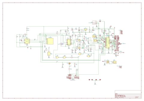
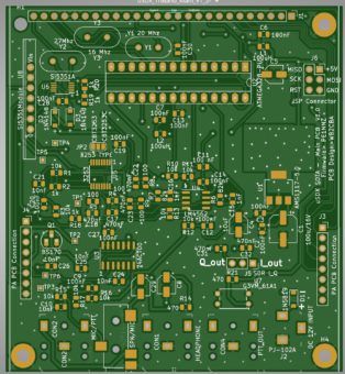
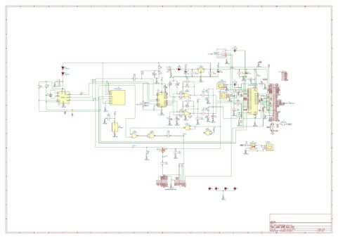
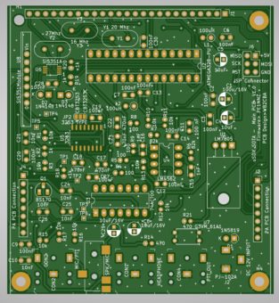
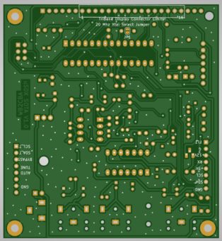
Here are schematic and PCB layouts of uSDX SOTA Main Board:
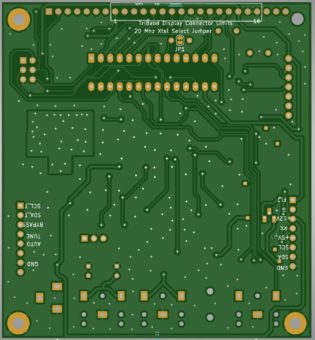
Component side layout:
Solder Side Layout:
This is smd parts finished Main Board:
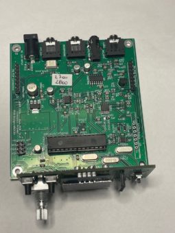
And this is main board with all parts soldered in to give an idea how the finished main board will look like:
Main Board schematic, pcb layouts, smd pcb production files which also include smd parts BOM , centroid pick and place file and pcb gerber file can be found in uSDX SOTA Main PCB.zip file.
Here is a BOM list of Through hole parts needed to complete uSDX SOTA Main board:
– 1 x Atmega328P microcontroller with Arduino bootloader flashed – There are online sites that are marketing ATmega328p microcontroller ready with Arduino bootloader flashed. Here is an example from amazon:
https://www.amazon.com/risingsaplings-2pcs-ATMEGA328P-PU-bootloader-Socket/dp/B08WWW75B2/ref=sr_1_13?crid=CMSNIM7N8O5F&keywords=arduino+bootloader-programmed+chip+atmega328p&qid=1636660774&qsid=133-7329843-9781304&sprefix=atmega328p+with+arduino+boot%2Caps%2C512&sr=8-13&sres=B01FQ1YU8K%2CB01KH54A6C%2CB00E87VWQW%2CB07R9VWD39%2CB07HRM2L3M%2CB07GPPK4DK%2CB01FQ8FKOG%2CB07JJX961X%2CB08915GQ89%2CB08WWW75B2%2CB07KK367N8%2CB01DLIJQA2%2CB00KM6ZA9I%2CB07G99NNXL%2CB08LNBYLBT%2CB0885RKVMC
– 3 x SJ1-3523N – 3.5mm audio connector – Digikey part nr: CP1-3523N-ND
– 1 x SJ-43514-SMT-TR – 4 pole 3.5 mm SMT Audio Jack – Digikey part nr.: CP-43514SJCT-ND
– 1 x 20mhz HC-49/US Crystal
– 1x 27mhz HC-49/US Crystal
– 1x16mhz HC-49/US Crystal
– 1 x BS170 Mosfet
– 1 x 28 pin DIP IC Socket
– 1 x 2.1mm x 5.5 mm DC Barrel Connector (THD)
– 1 x 2×3 pin ISP header male
– 2 x 8 pin male header
– 1 x 3 pin SDR OUT male header
– 1 x optocoupler OMRON G3VM-61A1 – Mouser part nr.:653-G3VM-61A1
Putting together uSDX SOTA Main board:
– I added a short tutorial guide on how to order boards from JLCPCB for smt pick and place at the bottom of this blog. Using this guide anyone can order uSDX SOTA boards from JLCPCB all smd parts installed.
– Ofcourse for brave hams with smt soldering skills the only thing you need to order is main board pcb with the gerber files included in production files folder. For the smd parts again in production file folder there is a BOM excell sheet . The last column is LCSC parts column. LCSC is basically Chinese equivalent of Digikey or Mouser. All you have to do is to enter LCSC site www.lcsc.com and enter the part designation starting with C letter in their search and you’ll get the part’s details that is used in smd production which you can order from Digikey or Mouser for your soldering skills!
– Some useful tips and details about SOTA Main Board
– SOTA Main Board has two different Crystals, a 16 Mhz and a 20 Mhz crystal. The reason for that is to allow programming the Atmega328p with standard 16Mhz Arduino bootloader onboard with USB interface. No need for 20 mhz bootloader. The slide switch in the display boards select these crystals. in PROG position 16 mhz Crystal is active and uSDX SOTA transceiver can be programmed as an ordinary Arduino uno board. In CAT position 20 mhz crystal is active and runs uSDX in it’s convenient operation frequency of 20 Mhz.
– 3253 IC type is now flexible on Main board and can be chosen with a jumper selection. JP2 jumper can select between 74CBT3253 and 74CBT3253C type. This jumper connects the unused switch to ground or VCC depending on type of 3253
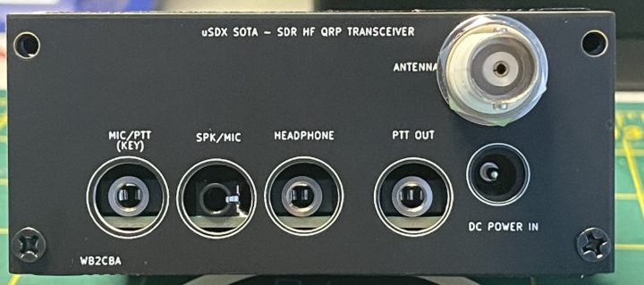
– 3.5 mm Jack pin outs:
– Headphone Jack:
– Headphone connector is 3.5 mm standard TRS jack.
Tip – Audio out
Ring – Audio out
Sleeve– GND
– This jack audio output is lowered with a 470 ohm resistor to suit feeding straight into PC mic input, earphones etc.
– MIC/PTT(KEY) Jack:
– This jack is also 3.5 mm standard audio jack in TRS combination.This jack also doubles as CW key input jack.
– In MIC/PTT INPUT MODE:
Tip – Mic input
Ring – PTT
Sleeve – GND
– In CW KEY INPUT MODE:
– Tip- DAH
Ring- DIT
Sleeve – GND
– SPK/MIC Jack:
– This is a 4 pole jack configured as TRRS.
– This is used to connect a hand Speaker/Microphone combination and uses BAOFENG UV-3R handheld cheap speaker/microphone similar to this one:
https://www.ebay.com/i/401863211871?chn=ps&norover=1&mkevt=1&mkrid=711-117182-37290-0&mkcid=2&itemid=401863211871&targetid=1068323860270&device=c&mktype=pla&googleloc=9003562&poi=&campaignid=10459841961&mkgroupid=104612009980&rlsatarget=pla-1068323860270&abcId=2146002&merchantid=6296724&gclid=CjwKCAiA25v_BRBNEiwAZb4-ZRvy1rwtRGU3fC6uOA1VcBckiyfsw1ZDwmYpcbaxb-eFdBSkii7VZRoCYVgQAvD_BwE
– Connection points are as follows:
TIP :SPEAKER
RING 1:MIC
RING 2:PTT
SLEEVE: Gnd
– PTT OUT Jack:
– This jack uses 3.5 mm standard audio jack. With the Solid state relay an external relay can be activated when PTT is pressed. This SSR is connected to port pin 11 of Atmega328p and needs to be activated from uSDX firmware. This pin can be controlled to delay TX when PTT is pressed so that external RF Power Amplifiers can be triggered on before TX.
– PTT Jack out pins:
TIP :OUT pin of SSR to external device (Pin 4 of SSR)
RING: OUT pin of SSR to external device(Pin 4 of SSR)
SLEEVE: GND(Pin 3 of SSR)
– uSDX SOTA Main Board is backwards compatible with uSDX TriBand displays to be used in uSDX TriBand configuration. To achieve this, do not install 16 Mhz crystal and solder JP1 to activate 20 Mhz crystal in uSDX TriBand configuration to use with uSDX TriBand Newhaven LCD or 2×16 Standard LCD boards. Also install the uSDX TriBand display boards in the limit shown on solder layout of Main board pcb display connector. uSDX TriBand displays do not incorporate slide switch for programming and no 16mhz crystal so no usb programming or CAT functionality!
uSDX SOTA Power Amplifier and Low Pass Filter Modules, (PA/LPF Boards):
In uSDX SOTA we can use any of those 3 options of power amplifier/Low pass filter boards which were also designed for uSDX TriBand.
Option 1:
uSDX OCTOBAND, 8 band PA+LPF Board released for using with uSDX TriBand design and can be used in uSDX SOTA or uSDX SOTA ATU configuration transceivers and fully compatible.
Here is the link for uSDX OCTOBAND PA+LPF blog article detailing how to build one:
https://antrak.org.tr/blog/projeler/octoband-usdx/
Option 2:
uSDX QuadBand, 4 Band PA+LPF Board THD released for using with uSDX TriBand design can be used in uSDX SOTA or uSDX SOTA ATU configuration transceivers and fully compatible.
Here is the link for uSDX QuadBand PA+LPF blog article detailing how to build one:
https://antrak.org.tr/blog/quadband-4-band-palpf-board-for-usdx-triband-an-all-mode-hf-qrp-transceiver/
Option3:
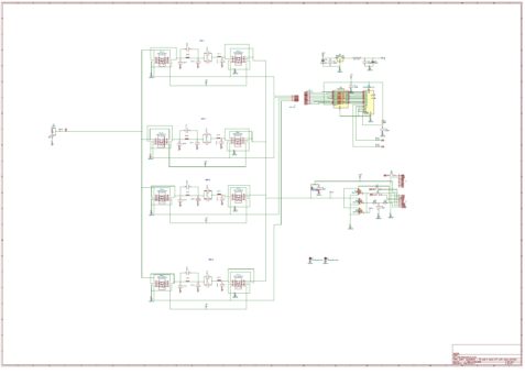
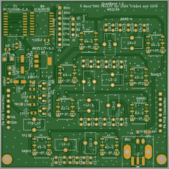
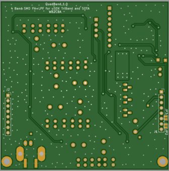
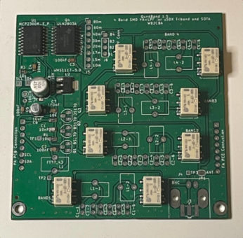
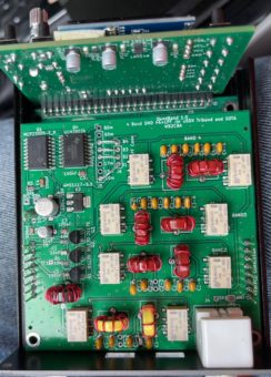
This option is a new pcb design which is actually a copy of QuadBand THD pcb with smd manufactured parts for ease of build.
Here is QuadBand smd board:
Component Layout of QuadBand smd:
Solder Layout of QuadBand smd:
QuadBand smd parts installed board:
QuadBand all parts installed board:
QuadBand smd Board PDF of schematic, pcb layouts,smd pcb production files which also include smd parts BOM, centroid pick and place file and pcb gerber file can be found in uSDX SOTA QuadBand SMD PCB.zip file.
Here is a BOM list of through hole parts needed to complete uSDX SOTA QuadBand board:
– 3 x BS170 Mosfet
– 1 x BNC THD antenna connector – Digikey Part Number:ARF1690-ND
– 1 x 100uH rf choke – Digikey part number: 118-5300-25-TR-RCCT-ND
– 1 x FT37-43 Toroid with AWG24 wire 20 turns.
– 2 x 8 pin female header
– 4 x Band LPF parts (capacitors and Toroids for each desired and selected band by the user)
kitsandparts.com is a great source for Toroid cores.
Some useful tips and details about SOTA QuadBand smd PA+LPF Module:
– All relevant build information and Low pass filter parts selection is similar to Through hole design QuadBand PA+LPF board which I released as a detailed build blog in this link below:
For all details and build guide please refer to this link to build QuadBand PA+LPF smd board.
To keep this blog simple I am not going to repeat all those details here.
https://antrak.org.tr/blog/quadband-4-band-palpf-board-for-usdx-triband-an-all-mode-hf-qrp-transceiver/
– As you all will notice there is one difference between Through hole PA+LPF boards and this smd PA+LPF board, QuadBand smd PA+LPF has it’s own 5 volts voltage regulator on the board. The reason is that to distribute power and heat management between each module.
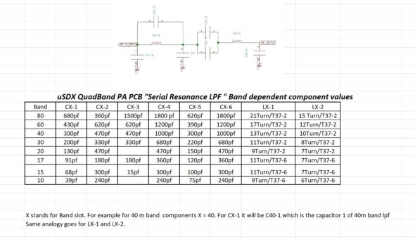
– For choosing band capacitor and Toroid values and details this table can be used:
– QuadBand SMD PA+LPF board contains four band LPF banks which means we can install only for bands. These bands can be any of the 8 bands chosen from above table.
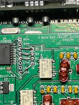
– After choosing our bands and installing each of the preferred LPF banks now we need to digitally connect those LPF banks to correct band selection outputs by short jumpers.
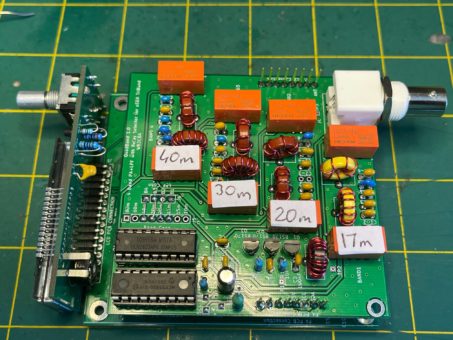
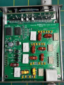
First it is good practice to mark out with little stickers which band bank occupies which chosen band like in this photo:
I installed on purpose higher frequency bands close to antenna starting with 10m then the next lowest frequency goes to the next band bank slot etc.
Let’s take my lpf board as an example how to connect band vs bank jumpers. My first LPF bank is 10m then bank 2 occupies 20m, bank 3 is 30m and bank 4 is 40m band. Now when we look at below photo 10m jumper goes to B1 which is 10m band, 20m jumper goes to B2 which is 20m band, 30m jumper goes to B3 which is 30m band and finally 40m jumper point goes to B4 which is bank 4 and populated by 40m band LPF parts. Now when we select a band associated relays will automatically and in correct order select each band LPF. Be careful on one important point when operating the rig: As we have only four bands and the other unpopulated four bands can still be selected and shown on display though there won’t be any LPF connected to them. So DO NOT TX on bands other than what bands are on your LPF board. Otherwise you can smoke your finals!
– QuadBand smd PA+LPF board is backwards compatible with uSDX TriBand Design and can be used similar to other through hole parts PA+LPF boards in TriBand design too.
IMPORTANT NOTE: To use any of those Power amplifier + Low pass filter boards with uSDX SOTA Transceiver, configuration Jumpers JP2,JP3 and JP4 on solder side of all PA+LPF boards needs to be soldered to close electrical connection of I2C signals and +5V power to header pins! Otherwise control signals from uSDX SOTA Main board won’t reach all these PA+LPF boards to switch band relays. DO NOT SOLDER JP1 ANT!
uSDX SOTA 128×64 OLED Display board:
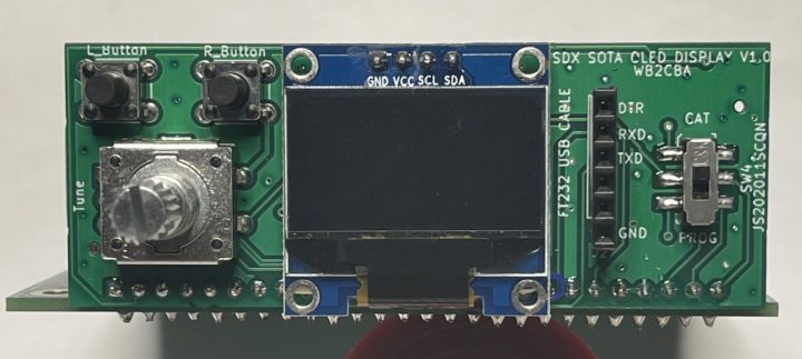
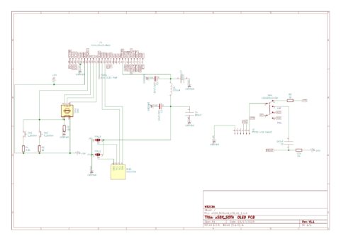
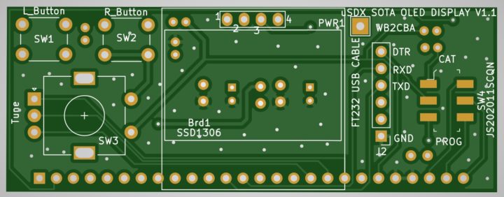
Here is uSDX SOTA OLED Display Board:
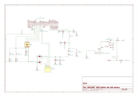
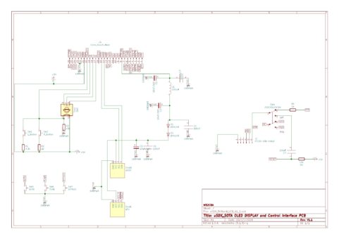
Schematic:
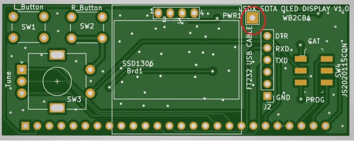
Display side layout:
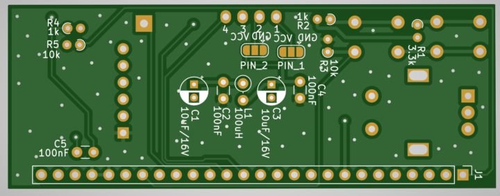
Component Side Layout:
uSDX SOTA 128×64 pixel 0.92” OLED Display Board incorporates a rotary encoder for tuning and menu selection functions, two tactile push button switches for menu and other functions to operate the rig. Also an smd slide switch to select between CAT and USB programming modes. The basic function of this switch is to alternate between two microcontroller crystals depending on chosen function. If we want to program ATmega328p with a new uSDX firmware then we choose PROG with slide switch which connects 16Mhz crystal to the system. Also connects reset pin to DTR which is needed by Arduino IDE to reset ATmega328p for programming. Programming is similar to any Arduino uno programming.
When we are done with programming then slide switch is positioned in CAT position which switches crystal to 20 Mhz normal operation speed of uSDX. This switch also connect DTR pin of USB interface to PTT pin of ATmega328p which in turn is used for full CAT PTT functionality. All of this will be explained later in this blog in detail.
uSDX SOTA does not have a USB to TTL converter chip built in. Instead has a FTDI cable pin layout header to connect a FTDI USB to TTL cable or adapter which can be found online for as low as 2 US Dollars. Main reason not to have an onboard USB to TTL IC is that chip shortage and possible interference to RX in some models of these chips. I found out that having an external USB to TTL adapter cable or adapter board had no RF noise interference.
Here is a link for FTDI Cable:
https://www.amazon.com/dp/B00DJBNDHE/ref=cm_sw_r_wa_api_glt_fabc_G4TSWT4TXZT05GP2H5YY
And link for FTDI Adapter:
uSDX SOTA OLED Display Board files are in uSDX SOTA OLED DISPLAY.zip
BOM List for THD parts to complete building uSDX SOTA 128×64 OLED Display Board:
1 x Rotary Encoder – Digikey Part Number: PEC11R-4015K-S0024-ND
2 x 6mm lever with 6mm x 6mm footprint tactile switch
1 x SMT DPDT slide switch JS202011SCQN – Digikey Part Number : 401-2002-1-ND
1 x SSD1306 128X64 Pixel 0.92” OLED Display
1 x 26 pin 90 degrees male pin header(Display connector)
1 x 6 pin female pin header(USB to TTL Interface connector)
TIPS on building OLED Display board:
There are two important points we need to pay attention:
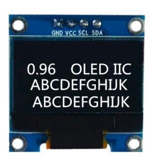
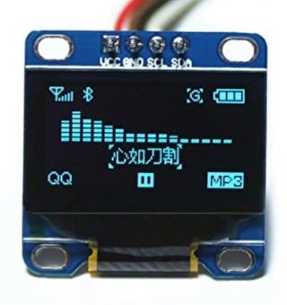
1- Choosing jumpers for VCC and GND supply pins of OLED Display. This is important as 128×64 OLED displays come in two different VCC and GND pin orientation. As in the photos below:
Top OLED has GND as pin 1 and VCC as Pin 2 and the bottom OLED has VCC as Pin 1 and GND as Pin 2.
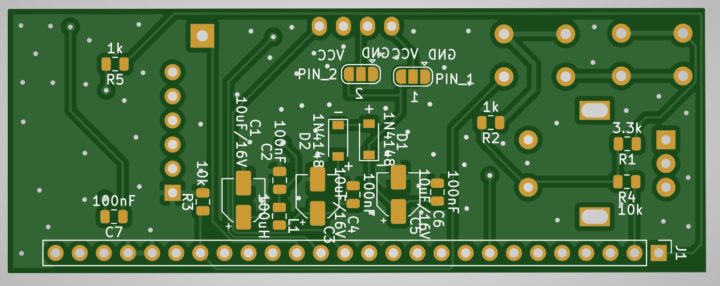
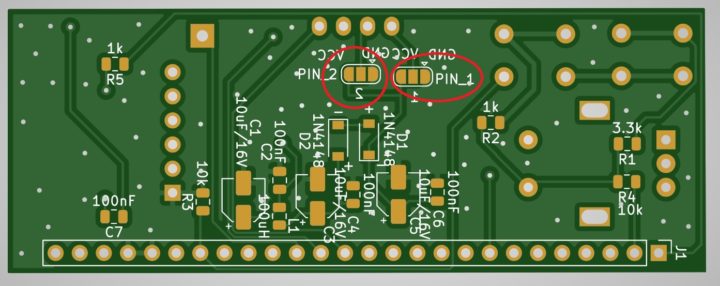
To choose the correct pin combination to match the OLED display chosen I added two solder jumpers:
These Jumpers correspond to Pin1 and 2, VCC or GND position. For example if we selected an OLED Display with pin 1 = VCC and Pin 2 = GND then Pin 1 jumper should have a solder blob between VCC and 1 and Pin2 jumper should have solder blob between GND and 2. Now we are set as pin 1 VCC and Pin 2 GND. Same applies to GND/VCC version of oled display opposite of what we did on soldering jumpers.
2 – Modifying OLED Display to reduce RF interference:
OLED displays are notoriously RF noisy due to their DC capacitive charge pumps which produces all kinds of spikes. To get rid off this noise I devised a simple modification.
Step 1 – get rid off charge pump capacitors C3 and C4. This is actually very easy. Heat up your soldering iron around 400C and heat up those two caps until you can lift with a pair of tweezers. After that we will need to solder a short wire of 20 to 25mm(around an inch) to C6 as in the photo below.
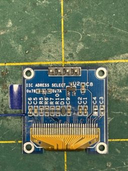
For Soldering and building OLED Display for uSDX SOTA start with THD components and 90 degrees header soldering. After all Through hole components are soldered in now we can solder modified OLED display. Attach a tiny double sided tape to hold OLED display in place also raising it couple of millimeters.
There is a square pad on right side of oled display. Now align that cable we soldered so that it comes out towards that side of PWR1 pad. After soldering OLED display in place solder that short wire that comes out from C6 cap of OLED display to this square soldering pad named as PWR1. This is where oled display gets it 12V refresh voltage.
So what’s the story here! OLED displays are powered with 3.3 volts but it needs between 7V and 15V to drive OLED cells. Those charge pump capacitors help to produce that voltage from 3.3V. Of course this is an switching upverter which produces a lot of high frequency pulse which interferes with RX quality. By eliminating this charge pump we simply get rid off that unwanted interference by supplying 12VDC from TRX power input.
Here is a youtube video that I uploaded to compare between two cases, unmodified and modified OLED Display RF noise:
– One last tip: Slide Switch JS20211SCQN is a SMT slide switch and it is on the display side of OLED Display so it won’t be soldered by JLCPCB so we need to solder this switch by hand which is pretty easy to do. The reason why this smd device is not pick and place by JLCPCB is that they only place parts on one side of the pcb and this is on the opposite side of majority of smd parts.
uSDX SOTA ATU double 128×32 OLED Display Board:
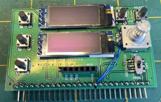
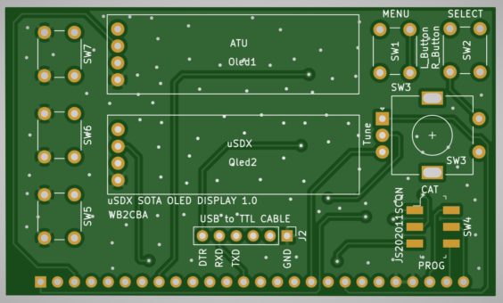
uSDX SOTA ATU display board is used in built in ATU uSDX SOTA TRX. This display board has two 128×32 OLED Displays, top one for ATU functions display and lower one is used for uSDX TRX functions display.
Here is complete uSDX SOTA ATU Display board:
uSDX SOTA ATU Display Board Schematic:
uSDX SOTA ATU Display side layout:
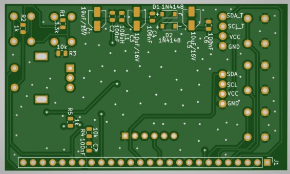
uSDX SOTA ATU Display component side layout:
uSDX SOTA ATU 2x128x32 pixel OLED Display Board incorporates a rotary encoder for tuning and menu selection functions, two tactile push button switches for Transceiver menu and mode functions and three tactile push button switches for Automatic Antenna Tuner operation. Also an smd slide switch to select between CAT and USB programming modes as in 128×64 OLED display.
The basic function of this slide switch is to alternate between two microcontroller crystals depending on chosen function. If we want to program ATmega328p with a new firmware then we choose PROG with slide switch which connects 16Mhz crystal to the system. Also connects reset pin to DTR which is needed by Arduino IDE to reset atmega for programming. Programming is similar to any Arduino uno programming.
When we are done with programming, slide switch is positioned in CAT position which switches crystal to 20 Mhz normal operation speed of uSDX. This switch also connects DTR pin of USB interface to PTT pin of ATmega328p which in turn is used for full CAT functionality.
uSDX SOTA ATU does not have a USB to TTL chip built in. Instead has FTDI cable pin layout header to connect a FTDI USB to TTL cable or adapter which can be found online for as low as 2 US Dollars. Main reason not to have an onboard USB to TTL IC is that chip shortage and possible interference to RX in some models of these chips. I found out that having an external USB to TTL adapter cable or adapter board had minimal RF noise interference.
Sample ink for FTDI Cable and FTDI adapter is above under 128×64 OLED display section.
uSDX SOTA OLED Display Board files are in uSDX SOTA ATU OLED DISPLAY.zip
BOM List for THD parts to complete building uSDX SOTA ATU Dual 128×32 OLED Display Board:
1 x Rotary Encoder – Digikey Part Number: PEC11R-4015K-S0024-ND
5 x 6mm lever with 6mm x 6mm footprint tactile switch
1 x SMT DPDT slide switch JS202011SCQN – Digikey Part Number : 401-2002-1-ND
1 x SSD1306 128X64 Pixel 0.92” OLED Display
1 x 26 pin 90 degrees male pin header(Display connector)
1 x 6 pin female pin header (USB to TTL Interface connector)
TIPS on building OLED Display board:
– Modifying OLED Display to reduce RF interference:
OLED displays are notoriously RF noisy due to their DC capacitive charge pumps which produces all kinds of spikes. To get rid of this noise I devised a simple modification.
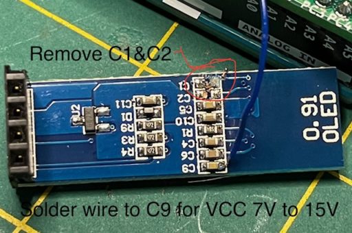
Step 1 – get rid of charge pump capacitors C1 and C2. This is actually very easy. Heat up your soldering iron around 400C and heat up those two caps until you can lift with a pair of tweezers.
After that we will need to solder a short wire of 50mm (around two inches) to C9 as in the photo below.
Modify both 128×32 OLED displays as explained in Step 1.
Step 2:
For Soldering and building OLED Display for uSDX SOTA ATU start with THD components and 90 degrees header soldering. After all through hole components are soldered in now we can solder modified OLED displays. Attach a tiny double sided tape to hold OLED displays in place also raising it couple of millimeters.
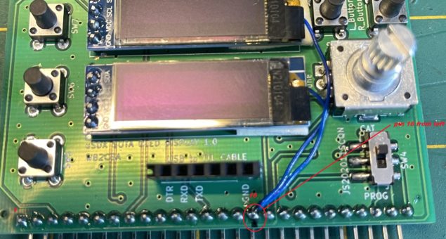
Now align those cables we soldered so that they extend out towards 26pin display header connector. After soldering OLED displays in place, solder both wires that comes out from C9 cap of OLED displays to pin 16 of display connector header. Pin 16 is is 16th pin from left side of OLED board when OLEDs are facing you. This is where OLED displays get their 12V refresh voltage.
So the story here is same as 128×64 OLED! They are RF noisy too! These OLED displays are powered with 3.3 volts but it needs between 7V and 15V to drive OLED cells. Those charge pump capacitors help to produce that voltage from 3.3V. Of course this is an switching upverter which produces a lot of high frequency pulse which interferes with RX quality. By eliminating this charge pump we simply get rid off that unwanted interference by supplying 12VDC from TRX power input.
– Slide Switch JS20211SCQN is a SMT slide switch and it is on the display side of OLED Display so it won’t be soldered by JLCPCB so we need to solder this switch by hand which is pretty easy to do. The reason why this smd device is not pick and place by JLCPCB is that they only place parts on one side of the pcb and this is on the opposite side of majority of smd parts.
– PUSH BUTTONS and Their functions:
– L_Button and R_Button are uSDX TRX buttons and they are used to select menu and exit from menu etc.
– SW5,SW6,SW7 are automatic antenna tuner unit buttons.
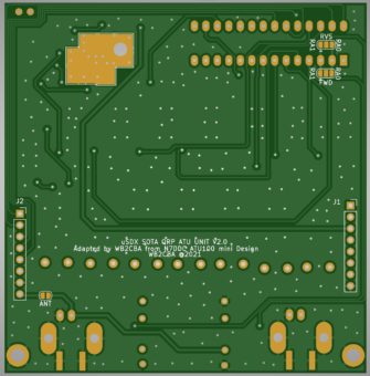
uSDX SOTA Automatic Antenna Tuner Unit (ATU):
Automatic Antenna Tuner Unit is a miniaturized clone of David Fainitski, N7DDC’s infamous 7X7 automatic antenna tuner unit adapted for QRP operation up to 10 watts.
uSDX SOTA ATU automatic antenna tuner unit files including production files and pdf schematic and pic16F1938 picmicro firmware hex file can be found in uSDX SOTA ATU.zip
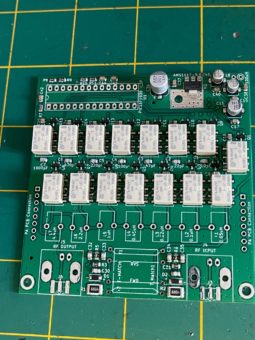
ATU smd parts installed board:
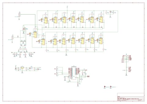
7×7 ATU Schematic:
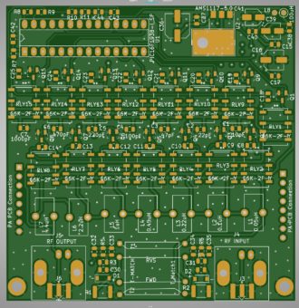
ATU component side layout:
uSDX SOTA ATU solder side layout:
uSDX SOTA Automatic Antenna Tuner Unit Through hole parts BOM List:
1 x PIC16F1938 – Pic microcontroller – Mouser Part Number: 579-PIC16F1938-I/SP
1 x 28 pin DIP IC Socket
1 x 100uH rf choke – Digikey part number: 118-5300-25-TR-RCCT-ND
2 x PCB type BNC THD Connector – Digikey part number: ARF1690-ND
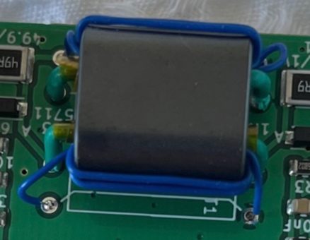
1 x BN43-202 Binocular core for tandem match – 3 x T37-6 toroid core
2 x T37-2 toroid core
2 x T50-2 toroid core
All toroid cores and BN43-202 binocular core can be outsourced from: https://kitsandparts.com/toroids.php
0.50 mm / AWG24 enameled inductor wire
2 x 8 pin female long leg headers ( Arduino stackable headers)
Example link for these headers:
https://www.sparkfun.com/products/9279
uSDX SOTA ATU – Automatic Antenna Tuner Unit building Tips:
– Start with soldering all Through hole components except Tandem match, toroid cores and stackable headers.
– Setting tandem match Jumper:
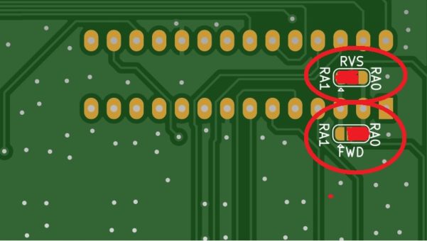
ATU has two jumpers on solder side of ATU pcb. These are called FWD and RVS. These jumpers are connection points for tandem match to A/D(analog/digital) input points to PIC16F1938 microcontroller. To be flexible for testing I left those as jumpers rather than connecting to A/D pins of Picmicro.
Here is how these jumpers should be soldered:
Solder only those areas highlighted with red filling.
– Winding tandem match binocular core:
Tandem match binocular core is the most important part of this ATU build and needs special attention and care for good operating results.
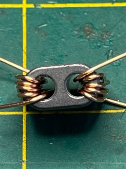
Each side of BN43-202 Binocular core has 5 turns. One turn means passing wire once inside the core. For 5 turns we need to pass 5 times. Use 0.5mm/AWG24 wire.
For straight through feedback wires inner core of RG-58 coaxial cable can be used. Any insulated wire will do the job actually.
Here is a photo of 5 turns wound tandem match:
When winding tandem match just be careful to start winding one side from bottom to top and adjacent core hole on same side start from top to bottom as in the above photo.
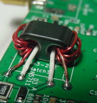
Here are photos of installed tandem match:
– Toroids and turns:
There are seven toroidal inductors that are acting as the L part of L/C tuning circuit.
Toroid types and turn values are listed below:
– L1 is a T37-6 yellow toroid with 4 turns of 0.5mm/AWG24 enamel wire.
– L2 is a T37-6 yellow toroid with 6 turns of 0.5mm/AWG24 enamel wire.
– L3 is a T37-6 yellow toroid with 9 turns of 0.5mm/AWG24 enamel wire.
– L4 is a T37-2 red toroid with 11 turns of 0.5mm/AWG24 enamel wire.
– L5 is a T37-2 red toroid with 16 turns of 0.5mm/AWG24 enamel wire.
– L6 is a T50-2 red toroid with 21 turns of 0.5mm/AWG24 enamel wire.
– L7 is a T50-2 red toroid with 30 turns of 0.5mm/AWG24 enamel wire.
Tips on TOROID winding:
– One turn means one pass of wire through center of toroid core.
– Always clean enamel coating from end of winding thoroughly. There is two proven methods to achieve this:
1- Heat end of wire enough so that all enamel coating burns up. Then soak with solder to cover that section.
2- Using cutting knife scrape enamel coating and then heat up for remaining residue then solder soak to have a shiny solder covered solder point. This is my go to method.
3- Always test with a continuity tester all is good and exposed before soldering and after soldering. After solder test works great with LPF toroids but not so much in ATU toroids as relays are shorting toroids! Beware!
At this point everything on ATU board should be soldered except the Arduino stackable headers. We will cover that part when we will put together uSDX SOTA ATU TRX rig below.
Programming PIC16F1938 picmicrocontroller with uSDX SOTA ATU firmware:
Programming picmicro PIC16F1938 may seem intimidating when compared to Arduino though it is fairly simple with right tools.
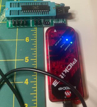
For this we need to invest on a PICKIT 3 programmer set like this one:
Sample link for a pickit 3 programmer:
These programmers are relatively cheap on ebay or aliexpress.
Now we need to download and install pickit 3 programmer software to run on Windows PC from this link:
ww1.microchip.com/downloads/en/DeviceDoc/PICkit3%20Programmer%20Application%20v3.10.zip
– Now setup your pickit3 programmer and adapter as in above photo and insert PIC16F1938 into ZIF IC socket as in the photo, pin 1 of picmicro all the way to the top edge ZIF socket.
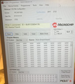
– Plug in USB cable to your windows PC and run PICKIT3 programmer software.
You should see a screenshot similar to this if all is good and your picmicro is detected:
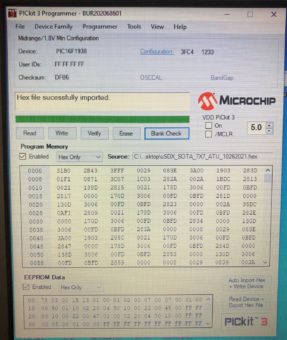
– Click on File and then click on import. Find uSDX_SOTA_7X7_ATU_10262021.hex file in your saved directory and click on it.
You should see that all program flash memory locations are filled with random hex values and also EEPROM data area will be filled with random hex values with “Hex file successfully imported” message as in below photo:
– Now click on Write button and wait until “Programming successful” message appears and then we are done with programming Picmicro. Insert programmed PIC16F1938 into it’s 28 pin DIP IC socket on ATU board. Now uSDX SOTA ATU module is ready to be installed in uSDX SOTA ATU rig.
– Heatsink for uSDX SOTA ATU:
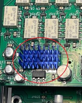
uSDX SOTA uses non latching relays which are on always so 5 volts voltage regulator can get warm. This is a precaution I am using. Tiny heatsinks with double sided silicon tape glued on regulator heatsink area as in the photo.
This is the link for these heatsinks:
This concludes building each LEGO module of uSDX SOTA HF modular Transceiver.
Now let’s build something useful with these modules called uSDX SOTA HF Transceiver!
1 – Bulding uSDX SOTA HF Transceiver:
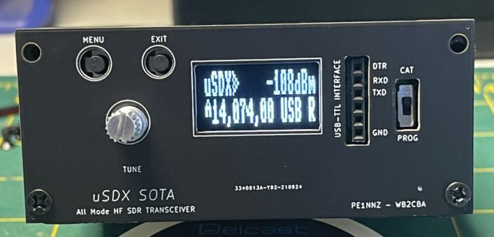
This transceiver is similar in appearance to uSDX TriBand Transceiver. Utilizes the same aluminum clamshell enclosure. Though now we have new face plates! Here is the uSDX SOTA FACE PLATES.zip file which contains these new face plates.
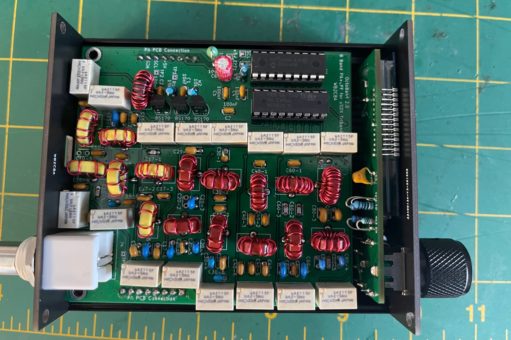
Finished uSDX SOTA Transceiver will look like this:
This version of uSDX SOTA transceiver will utilize these modules:
– 1 x uSDX SOTA Main Board
– 1 x uSDX PA/LPF Board – This can be Octoband or any of the Quadband PA+LPF boards.
– 1x uSDX SOTA 128×64 OLED Display Board
– 1x Front Face plate
– 1xBack face plate
– 100mm x 88mm x 38mm extruded aluminum enclosure.
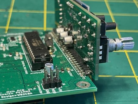
– First step is to solder OLED 128×64 display board to main board. Make sure that both boards are 90 degrees to each other as in photo and also pay attention how the 26 pin header is oriented. If it is not oriented like in the photo it won’t fit into aluminum enclosure!
Now Plug in preferred PA+LPF board in place. Slide in one half aluminum clamshell mainboard and PA+LPF assembly and bolt on front and back face plates to secure boards in place.
First thing first before testing! we need to program ATmega328p with latest uSDX firmware from Guido’s github repository.
These are the steps for this procedure:
1- Download latest firmware from this link:
https://github.com/threeme3/usdx/blob/master/usdx.ino
2- Open in Arduino ide and uncomment these two lines:(remove // )
#define OLED_SSD1306 1 // OLED display (SSD1306 128×32 or 128×64), connect SDA (PD2), SCL (PD3)
#define LPF_SWITCHING_WB2CBA_USDX_OCTOBAND 1 // Enable 8-band filter bank switching: non-latching relays wired to a MCP23008 GPIO extender on the PC4/PC5 I2C bus; relays are using GND as common (ground), GP0..7 used by the individual latches K1-8 switching respectively LPFs for 80m, 60m, 40m, 30m, 20m, 17m, 15m, 10m
3- Now comment these lines (Add // at the beginning of line) in order to save memory space of ATmega328p:
#define LPF_SWITCHING_DL2MAN_USDX_REV3 1 // Enable 8-band filter bank switching: latching relays wired to a TCA/PCA9555 GPIO extender on the PC4/PC5 I2C bus; relays are using IO0.0 as common (ground), IO1.0..7 used by the individual latches K0-7 switching respectively LPFs for 10m, 15m, 17m, 20m, 30m, 40m, 60m, 80m
If you get an error message stating that Arduino ide can’t fit program into memory then comment by adding //
//#define CAT 1 // CAT-interface
Now uSDX code will fit in but we lose CAT functionality. So my solution to this is to test the rig with this configuration and make sure all is working fine.
Now we can uncomment by removing //
#define CAT 1 // CAT-interface
And comment by adding // to:
//#define DIAG 1 // Hardware diagnostics on startup (only disable when your rig is working)
Now code will fit just fine into memory of ATmega328p and as we already tested our rig and all is good we don’t need any more power up diagnostics! This always worked for me without compromising any functionality of uSDX firmware options.
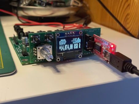
4- Connect FTDI pin compatible USB to TTL cable or USB to TTL adapter as in the below photo:
Match GND and DTR pins with corresponding GND and DTR pins on uSDX SOTA USB to TTL header!!!
5- Position slide switch to PROG position.
6- Power on uSDX SOTA TRX with external 12V DC. 5V USB is not used and connected for DC clash safety. External 12V DC needs to be connected and powering up uSDX SOTA Transceiver while programming. It is always a good safety precaution to plug in your dummy load just in case to antenna BNC to prevent accidental TX and smoking your finals!
7- Select Arduino UNO as board on Arduino IDE and program as programming an ordinary Arduino UNO board.
8- When uploading is done power off rig and push slide switch to CAT which will run the rig in normal operation speed and unplug USB to TTL adapter.
We are done with programming ATmega328p!
Now the moment of truth: Testing…
Now all pcbs are built, ATmega328p is programmed and ready to rock’n’roll, now it’s time to test!
To work through testing smoothly we need instruments! And here are these:
– A multimeter
– A bench power supply with 12V, 1 amps capacity at least and current limit is a great first start up benefit.
– A Frequency Counter with hertz resolution up to 30 mhz.
– A RF powermeter capable of measuring up to 10 watts.
– A dummy load up to 10 watts.
With these instruments it’s a breeze to work out adjustment and testing of this rig.
Here is a simple test procedure that I use:
1- Connect your dummy load at PA output.
2- Connect your power supply in series with current measurement mode on your multimeter. Use a second voltmeter if you have for observing voltage. Of course if you have a bench power supply with Voltage and Current displays then ignore these steps. Just connect your PSU to uSDX SOTA.
3- Limit your power supply current to 150 miliamps. Now power up and see how much current drawn on RX. It should be around 90 to 100 miliamps in RX.
4- Let’s say we are on 20m band so tune to USB 14000000 mhz in the lcd screen then enter menu by pressing left button and scroll up to menu item 8.1 Freq which is local oscillator frequency. Connect your frequency counter probe to SI5351 “0” output and ground connection. Now click rotary encoder once then rotate the encoder such that you see 14000000 mhz on your frequency counter. Don’t pay any attention to oled display of uSDX at this point. As you rotate your encoder your crystal frequency will change from initial 2700000 mhz. The trick is to match displayed frequency on frequency counter to SI5351 output frequency which is 14000000 mhz in our example by turning rotary encoder. If you see 14000000 Mhz on your frequency counter then it matches your local oscillator frequency by hertz. Now click left button once more to store and then click right button to exit from menu. You are done!
5- Now we will adjust RF power output. Set your power supply current limit to 1 Amps. Select the desired band. Plug in your microphone to MIC/PTT input and connect your rf power meter and a 10 watt minimum dummy load at RF power meter output. Now power up uSDX SOTA rig and Select CW mode with pressing right pushbutton(EXIT pushbutton).
Press left button and enter the menu area and scroll until 8.3 PA Bias MAX and lower that to 100. Then scroll to 8.2 PA Bias Min and scroll until 20.
Now press PTT and check your power output. If all is good then you should see something between 2.00 to 5.00 watts rf power output depending on your selected band.
Now record your power output with your current drawn at this output.
Now enter menu 8.3 PA Bias max and increase from 100 in increments of 10 and transmit in each increment to watch your rf output and current. If you are in a state that current is increasing but rf power is staying at where it is without significant increase then we are saturating the PA mosfets into inefficient zone so we need to roll back until rf power stays same but current decreases slightly. When we see RF power also roll back then we are set, leave it like that.
Now uSDX SOTA is ready for a qso!
Let’s build a uSDX SOTA ATU – A uSDX SOTA with built in automatic antenna tuner:
In order to put together ATU built in version of uSDX SOTA we will use those same building blocks and boards plus an ATU module and ATU dedicated display module.
Which modules we will need:
1- Main Board
2- Octoband or any of the Quadband PA+LPF boards
3- uSDX SOTA ATU Double 128×32 OLED display board
4- uSDX SOTA ATU – Automatic Antenna Tuner board
5- Front and back face plates
6- 100mm x 88mm x 38mm extruded aluminum enclosure
uSDX SOTA ATU Front and Back panel gerber files are here:
uSDX SOTA ATU Face plates.zip
Steps to build uSDX SOTA ATU version HF Transceiver:
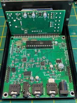
1- Solder Main board and uSDX SOTA ATU Display board. Make sure display board is 90 degrees to main board as in the photo below(watch out 26 pin display header orientation before soldering!):
2 – As PA+LPF board headers we will use Arduino 8 pin stackable female headers with long pins in uSDX SOTA ATU transceiver. This is important as we will stack ATU board on top of PA+LPF board.
3- Bolt on back face plate on to one half of the aluminum enclosure.
4 – Stack PA+LPF board on main board and slide it into it’s slot in aluminum enclosure half that we have installed the back face plate. Now bolt BNC connector so that it holds the whole board assembly.
5- Now stack on another 8 pin arduino stackable headers on top of PA+LPF header male pins. Now slide in ATU board BNC connectors out from their respective holes on back face plate while sliding and aligning header holes with stacked arduino stackable headers. Please see below photo:
Screw on BNC connector nuts of ATU BNC connectors to back panel so that ATU assembly is secure in it’s place. Now solder those Arduino stackable headers of ATU from top. We are done! Congrats you have just build a uSDX TRX with internal ATU!
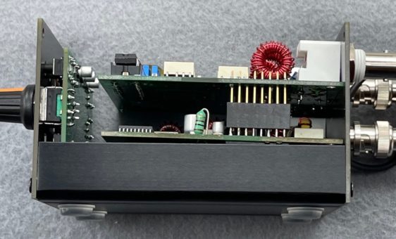
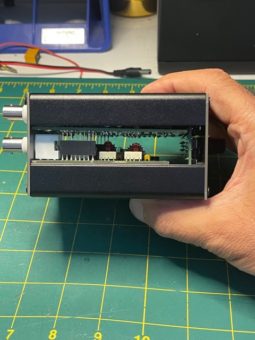
Now here is the pickle part! When we close the top half of aluminum enclosure that’s what we get:
There is a gap of 15mm/0.6 inch which can be covered with surplus pcb, plastic panels or 3D printed side panels. In my rig I used two pcb panels painted in black and bolt them on top half aluminum shell.
Now we need to connect TRX RF output of PA+LPF board to ATU RF input.
For this RF connection I used these short BNC cables from amazon:
So why there is two RF input and a short cable connection and no internal RF connection? To be able to use a 10 Watt or so external RF Power amplifier with this rig. This way TRX antenna out can be connected to external PA RF input and external PA RF output can go into ATU input. Also the PTT out can control TX activation of external power amplifier. This way we will still benefit out of that ATU! Work is in progress on a compatible RF power amplifier for this rig!
Programming with USB adapter and initial testing of this uSDX SOTA ATU version is similar to uSDX SOTA rig which I covered above so I am not going to repeat those procedures again here not to further clutter this long post.
Testing ATU is pretty straight forward, when we TX to a 50 ohm dummy load if all is good and in working order with the ATU we should see on the ATU display which is the top 128×32 OLED, RF input and RF output power almost equal to each other, SWR around 1.00 and EFF around 99%. If we get these results on ATU OLED display then ATU is working and healthy. The slight difference in SWR is related to the dummy load resistance variance mostly.
Using Internal ATU:
Internal ATU has 3 push buttons.
BYPASS – This is the BYPASS pushbutton which the name depicts is a bypass. Bypassing the ATU and RF input goes straight as RF OUTPUT without any active Tuning attempt. The ATU display will still show current un-tuned parameters as RF INPUT, RF OUT, SWR and Efficiency. When BYPASS is active on upper middle section of OLED display a “-“sign appears indicating that bypass is activated.
TUNE – This pushbutton is used for two purposes. If it is pressed momentarily it will reset tune parameters from memory. ATU always keeps in memory the last tune parameters to tune to the last known conditions.in reset active mode “RESET” will appear in OLED Display.
When TUNE is pressed long “TUNE” will appear in OLED Display. Now when PTT is pressed the rig will TX and ATU will automatically TUNE to lowest possible SWR condition with that antenna.
AUTO – This pushbutton activates AUTO tuning function. AUTO tune always attempts to re-tune if SWR condition is higher than SWR=1.3 during TX. This is a handy function when operating in contest conditions or CW and changing bands without worrying about manual re-tune. When AUTO is active a “.” appears in upper middle section of ATU OLED display.
This concludes going through all bits and pieces and tricks and hints of soldering and building these uSDX SOTA rig modules and putting together different type of uSDX SOTA SDR HF Transceivers with options for our taste and usage.
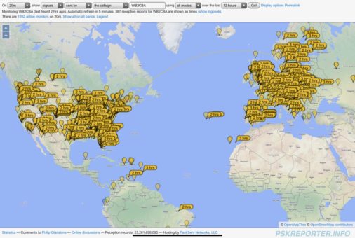
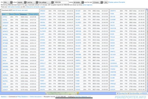
So does thing work??? Here is Pskreporter data of one of my QSO sessions on digital modes with uSDX SOTA ATU Transceiver in COTA(Car On The Air) conditions from my car with 20m Hamstick mobile antenna.
I uploaded couple of videos operating uSDX SOTA with ATU rig. Links for those youtube videos:
uSDX SOTA with Through Hole components version:
Before designing and manufacturing uSDX SOTA modules in smd I needed to verify that all worked on a through hole design of the same rig. These are PCB gerber files for uSDX SOTA Main board and uSDX SOTA 128×64 OLED board with Through hole parts. These through hole boards are identical to their smd board counterparts and all build explanations detailed above apply to these boards too.
I know there are avid DIY builders out there building their Transceivers from scratch with through hole parts so I dedicate these through hole parts board uSDX SOTA rig to those fellow hams.
With Octoband and THD Quadband PA+LPF boards added to these Main board and OLED display board combination a complete through hole uSDX SOTA rig can be built.
Here is schematic of THD Main board:
THD Main board component side layout:
THD Main board solder side layout:
All files you need to build this main board: uSDX SOTA THD MAIN BOARD.zip
This is schematic of THD 28×64 OLED display:
OLED THD display – Oled side layout:
OLED THD Display – Component side layout:
All files you need to build this 128X64 THD OLED Display board: uSDX SOTA THD 128X64 OLED DISPLAY BOARD.zip
uSDX SOTA SMT PCB boards JLCPCB ordering guide:
Now let’s talk about the most important subject! How we are going to get these SMD boards manufactured! Here is a short guide for ordering SMD manufactured boards from JLCPCB!
Surface mount parts might be intimidating for most of us. They need healthy eyes and steady hands to solder. This SMT pcb manufacturing service cures that problem by manufacturing PCBs and installing all smd parts on them in a controlled factory environment! An example of cost for this service: uSDX SOTA Main board will cost you less than 15 US Dollars each for a batch of 10 PCB orders including DHL shipping! This means a PCB with 85% of parts assembled including that SI5351 beast! The trick is the more units of pcb you order the less you pay for one pcb in cost.
The reason for that is there are certain one time fee costs JLCPCB adds to their invoice. Those are SMT setting up fee, extended parts fee etc. These are one time cost charges for each pcb order batch. So if we order 5 pieces of pcb that surcharge cost will be shared by 5 pcbs. If we order 30 pcbs then that surcharge will be divided by 30 and will be less per pcb. That’s why it is always order pcbs in larger quantities as a group buy. Ok how we will do this smt ordering business!
I’ll explain this as simple as possible in steps:
1- We will need Production files:
In order to place an order a SMT manufactured PCB from JLCPCB we need three files
– GERBER file (contains all the files to manufacture the PCB board itself)
– BOM File(contains all smd parts, their smd footprints and JLCPCB stock numbers for each part)
– Foot print position file (it is also called as centroid file – coordinates of each smd part on the pcb for pick and place robot)
All these files are included in each boards ZIP file under production file directory.
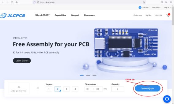
2- Create an account on www.jlcpcb.com. Follow instructions on their site.
3- After creating your account with all your credentials click on instant quote button
4- This will bring us to gerber file upload page. Click on add gerber file and upload your uSDX SOTA PCB’s gerber file from that pcb’s production files folder
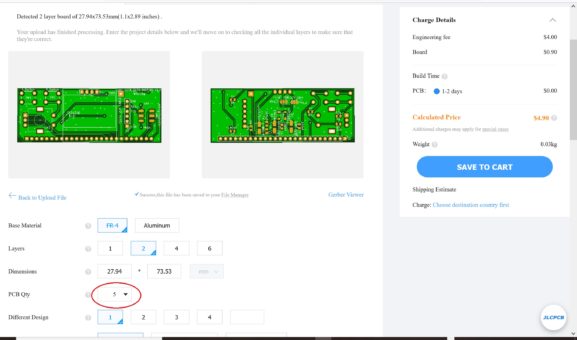
5- After uploading your gerber file you will see component and solder side images of your pcb. Now you need to choose how many pcbs you will order in quantity. The minimum is 5 pcbs.
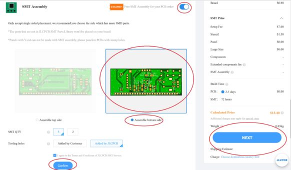
6- Now scroll down the same gerber upload page until you see the Free SMT Assembly for your PCB slide switch which should be light grey inactive position. Now slide it to activate. You should see below screen with top and bottom sides of your PCB. In this case I used uSDX SOTA 128×64 OLED Display as an example. In this display smd populated side is bottom side so I chose assemble bottom side. Now without touching anything else first click on Confirm then click on NEXT.
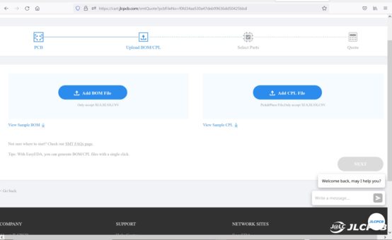
7- Now we will come to this next screen after clicking on NEXT. This is where we upload our BOM file and footprint position file which is marked as CPL button. These files are in your PCB’s production files. First click on Add BOM File button and upload BOM file from production files folder. Then click on Add CPL File Button and upload your footprint position file from your PCB’s production files.
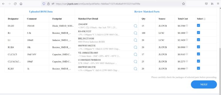
8- After uploading BOM and CPL files this is the screen which shows all the components of our PCB for SMT manufacturing. This table will show all the component part numbers, total number of each component that will be used for the whole batch of PCBs. Also total cost of each part for the whole batch of PCB order.
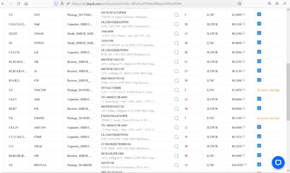
The most important column in this table is those blue check marks. If you see a blue check mark then it tells you that they have your components and those components have enough stock to manufacture your boards! If one or more parts is not in stock which can happen nowadays as there is chip shortage going on you might get an inventory shortage warning in place of blue check mark. Now JLCPCB does not have that part in stock and can’t pick and place that part and that part will be omitted from pick and place manufacturing. It’s not the end of the world! You can still get your pcb manufactured and hand solder those parts when you receive your pcbs.
Here is an example for that:
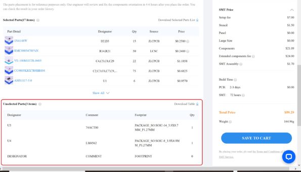
This is parts list for uSDX SOTA Main PCB. Two parts, 74ACT00DWR and LM4562 is out of stock. The rest of the parts are in stock so no problem with them. We will just order the PCBS and hand solder those parts afterwards. They are easy to solder smd parts.
Now click on NEXT to go to the next ordering screen.
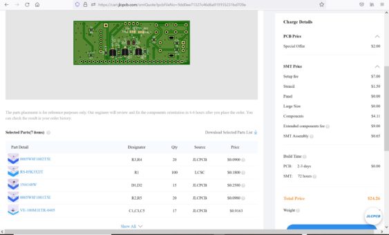
9- This is the next screenshot you will come across which shows your PCB and virtual pick and place finished product layout of your pcb. There might be orientation errors in this PCB virtual parts layout time to time, don’t worry about that. JLCPCB will review your pcb layout and pick and place file and then match those positions. After you ordered your PCB for SMT manufacturing they will review it and correct those mismatches. After this review when you access your account you will see a DFM file icon. If you click on that it will show your previous and manufacturing virtual corrected layout.
Ok as you will see all is good in this screen. There are 7 parts per pcb and all are selected, none of them left out due to stock shortage issue. Also you can see all those fees and one time charges etc in the right side of this screen. If you are happy with the prices and all then now we can add your pcb order to CART by clicking on save to cart.
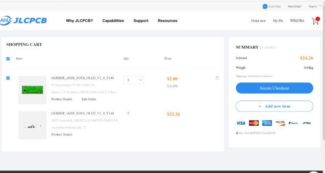
This CART screen will show your total cost for that ordered pcb batch. Now press on secure checkout and follow the procedure by verifying your address then shipment type and then payment etc.
Now let’s talk again about our nightmare case where some of the parts were out of stock!
In uSDX SOTA Main board PCB case two parts were out of stock and we still advanced the order and clicked next. Now as outlined in red box those parts are out of production and not listed on main parts list and will not be shown on virtual smt mounted pcb layout. We can still go ahead with the order and save to cart and get main board pcbs manufactured and when we outsource those parts we can hand solder them. It’s not the end of the world!
Personally I encourage fellow DIY lover hams to give it a try on ordering uSDX SOTA boards smt manufactured from JLCPCB. You will be surprised how cheap they will be for an order of 10 boards. Even with minimum 5 boards is reasonable price. The biggest benefit is that 85% of the transceiver rig is coming to your door step already soldered in!
FINAL WORD and Thank you:
I started this uSDX pcb design frenzy on March of 2020 on COVID-19 mandatory lockdown and here we are with uSDX SOTA modular HF Transceiver! With this final uSDX design, especially with uSDX SOTA ATU I achieved what I was dreaming for, A DIY QRP portable SOTA rig adaptable to any antenna condition thanks to it’s built in ATU! This is my dream come true!
I can’t thank enough Guido Ten Dolle, PE1NNZ for his brilliant uSDX Arduino firmware! Without it I could never achieve this.
I sincerely thank my friend Ken Delap, KX9U for his support and endless efforts in building and testing my uSDX prototype boards! Diving into rabbit holes with me in this project that sometimes led to nowhere!
I would like to thank Manuel Klaerig, DL2MAN for his contribution and being cool about my shameless copies of his excellent PA/LPF board designs.
I also would like to thank David Fainitski, N7DDC for his excellent ATU-100 Automatic antenna tuner and having it open source for ham world. Without his ATU design I couldn’t achieve my goal.
Last but not least I would like to thank Ham radio community and https://groups.io/g/ucx/topics uSDX group for their support and vast knowledge on uSDX eco system.
I am releasing uSDX SOTA design material to be open source and free for ham community to embrace and enjoy DIY building or commercially selling.
Anyone want to commercialize and sell uSDX SOTA Transceivers as modules or as a semi kit or as a full kit are allowed to do so under these terms:
– Commercial seller can not alter design and has to keep it in it’s original published form.
– Recognition of uSDX SOTA originators and designers PE1NNZ and WB2CBA for their work on their site.
Barb – WB2CBA
NY 11/11/2021
wb2cba@gmail.com

