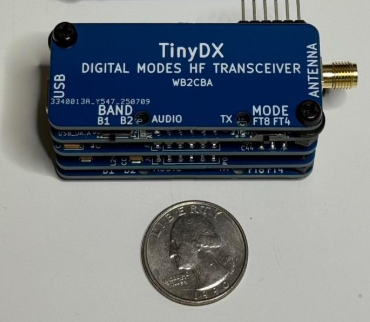
TinyDX – My Quest For Designing The Smallest Digital Modes HF Transceiver
For almost two years I am operating with QRPp Sub 1 Watt rigs I designed on FT8 and FT4 and I am obsessed with ultimate portability. The beauty of operating with sub watt rigs is that DC power requirement of this type of transceiver is well within standard USB power range. QRPp Sub Watt Transceivers can be powered by a Phone/Tablet or PC USB which is a huge advantage as we don’t need to carry a separate battery or power source when portable.
In the past I designed Credit Card sized transceivers such as ADX UnO. These are power hungry and still big for my portable quest.
I needed something way smaller, no extra power source and no PC or laptop to carry to operate. Just my phone! After some head scratching and brain storming I came up with TinyDX idea. DX stands for Digital Xceiver.
The challenge was to cramp an audio codec chip, an Atmega328P microcontroller, a SI5351 PLL VCO, a QSD Receiver with 3253 chip, an opamp , RF Power amplifier designed around a TTL chip, 5 band Low Pass Filter and all associated passive components in 2 inches(50 mm) by 1 inch(25mm) by 1.2 inch(30mm) space!
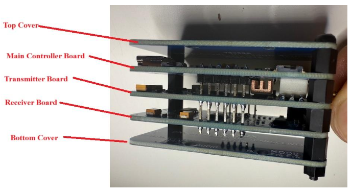
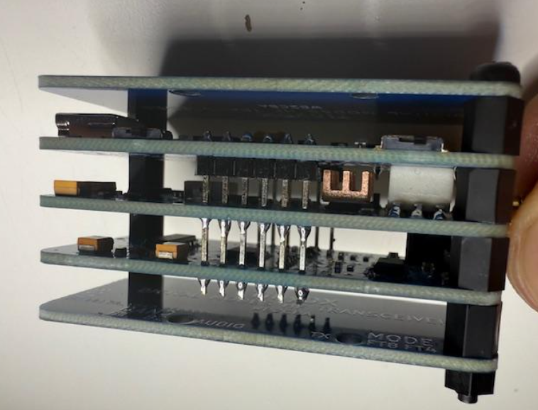
In order to achieve this, I came up with modular board design that will be stacked on top of each other and sandwiched between two pcb plates acting as a protective cover.
Here we can see all stacked modules:
Before we dive into analyzing bits and pieces of TinyDX let’s talk about specs:
- It’s a Two Band TRX in default band config of 20m and 15m.
- Though can operate on any of two of these bands configured in firmware, 20m/17m/15m/12m/10m.
- RF Output Power – 20m = 900 mW, 15m = 700 mW.
- Can operate on FT8 and FT4 modes in all 5 bands listed above.
- Operates on 5V USB power. Max current draw on 5V is 350 mA on TX, 100 mA on RX which is well within USB Power management limits.
As mentioned above TinyDX consists of three modules, Controller, Transmitter and Receiver.
Let’s go into details and working principles of each of these modules.
(Better resolution schematics of each module is TinyDX Github page: https://github.com/WB2CBA/TinyDX—Tiny-Digital-Modes-HF-Transceiver)
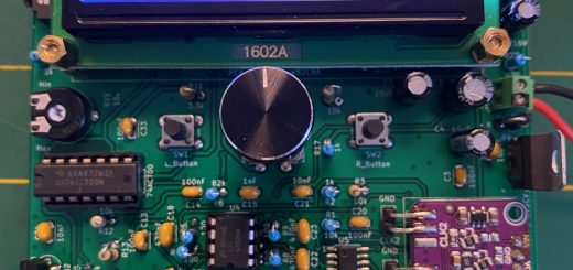
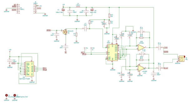
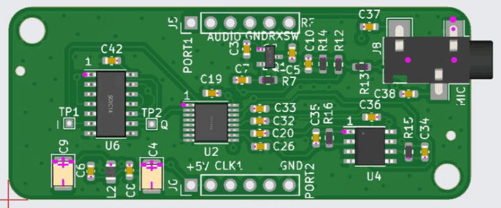
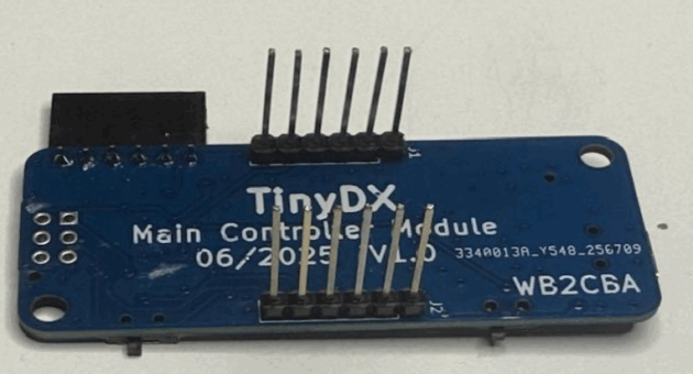
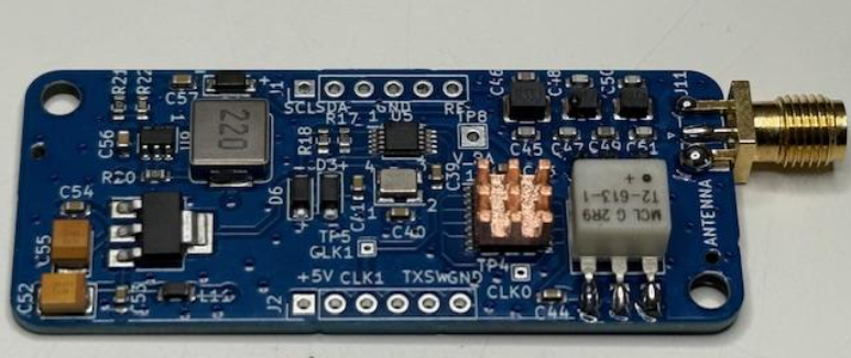
Audio Codec and Controller Module aka Main Module:
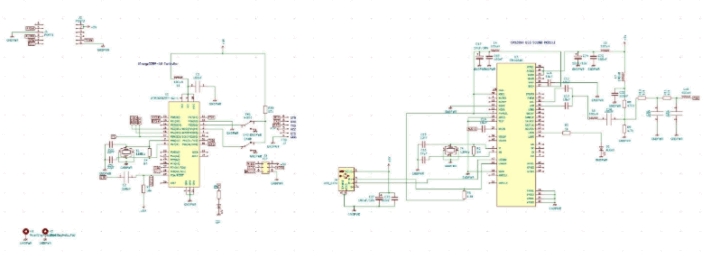
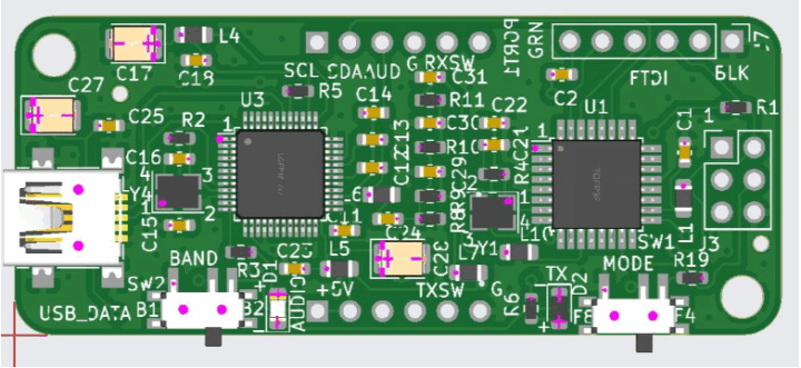
Main Controller module holds Audio Codec IC, CM108B and Atmega328P/AU Microcontroller. Also USB input connector for DC 5V power for the whole TRX plus Band Select and Mode select slide switches. I used miniature SMD slide switches to keep the board layout as small as possible.
Connection between all three modules of TinyDX is achieved by 2 x 6 pin 2.54 mm pin spaced headers located on each side of the module pcb.
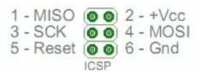
In Main Controller module we have a 2×3 pin header for standard Atmega ISP – In System Programming – interface. This ISP header interface is used for initial Arduino Uno bootloader upload. After Arduino Uno bootloader is uploaded TinyDX will appear in Arduino IDE as a standard Arduino Uno board to compile and upload firmware.
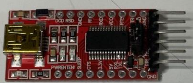
TinyDX does not contain a USB to Serial interface chip. This is on purpose to keep things simple and tiny as space is limited. Instead, a FTDI style USB to TTL adapter header is added. With an USB adapter like the one in below photo all firmware uploads can be achieved easily via Arduino IDE and serial port.
Here is a link for similar FTDI adapter: https://a.co/d/g4zegI2
Receiver Module:
TinyDX Receiver module consists of three main sections or parts,
- TX/RX Switch gate Mosfet
- 74ACT74 – Divider/I/Q Phase signal generator
- 74CBT3253PWR/LM4562 – QSD Tayloe Detector and I/Q Phase signal amplifier
Let’s dive into RX in detail.
- RX/TX switch is a simple mosfet switch which blocks any high-power signal coming from TX and switches on and passes any signal on RX. I used BSS123 small signal mosfet instead of BS170 which is most commonly used standard mosfet in these kind of QRP rigs. Advantage of BSS123 is high drain-source voltage of 100V compared to 60V of BS170.
- 74ACT74 is Dual D-Type positive edge triggered flip flop. In order to decode RX signals with QSD 3253 we need 90-degree phase difference two local oscillator signals which are called In-Phase(I) and Quadrature(Q).
These signals can be generated perfectly fine with SI5351 PLL VCO clock outputs though I find it easier and simpler to program a single Local oscillator clock and divide that clock by two and again two to obtain I and Q signals which are very stable and exactly 90 Degrees in Phase. This is the Pros of this method.
The Cons of this method is that we need to generate four times the RX target listening frequency. For example, if our target RX frequency is 14.074 MHz FT8 20m band then we need to generate 14.074Mhz x 4 = 56.296 MHz and feed that into the input of 74ACT74 divider which divides into four to obtain 14.074 MHz I and Q signals.
In-phase (I) signal form LM4562 opamp is fed to microphone input of audio codec chip CM108B and that’s it. So many will ask why to jump all those hoops and not perform a pure SSB Hilbert transform? Well, it’s a choice of simplicity with firmware effort. I wanted to have a pure DSB direct conversion Receiver, compared to SA612 or SA602, QSD Tayloe Detector is superior in narrow bandwidth and selectivity.
I find no difference in digital modes such as FT8 or FT4 any advantage of SSB decoding over DSB in my practical operation over the years with my designs using this particular choice. I am sure there will be many “Nay” sayers and I respect them though this my choice and works for me for such a simple and tiny transceiver.
I added a 3.5mm Audio out connector which can be used to access I/Q audio out signals.
Transmitter Module:
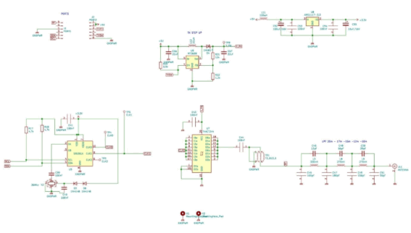
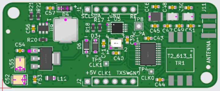
TinyDX Transmitter Module has three main sections:
- Power Supply
- SI5351 PLL VCO
- 74ACT244 RF Power Amplifier and Booster with 5 Band Low Pass Filter
- Power Supply module consists of two sections, a 5V to 3.3V LDO linear regulator which powers SI5351 PLL VCO with 3.3V.
- A Switching supply boost converter which boosts 5V to 7.0V to power 74ACT244 RF PA Booster. Now everyone will think that I must be crazy to power a TTL chip with 7.0V. Yes, I must admit it is unorthodox to push a 5V IC to its limits by powering it with 7.0V though 74ACT244 datasheet claims in Max ratings that is 7.0V.
A side note, on FDIM 2024 TTL Transmitter competition with this PA design powering 74ACT244 with 10.5V I achieved 1.8 Watts on 7 Mhz. This chip can tolerate a lot of abuse! - After boosting signal from SI5351 it’s fed into Mini Circuits T2-613-KK81+ transformer which is a manufactured bifilar transformer connected as auto transformer. This further boosts TX signal which is an ugly square wave style signal. After entering into Low Pass Filter it comes out as a pure sine wave without any significant harmonics.
Why a Mini Circuits transformer instead winding one? I get this question a lot. Simple answer is efficiency. No matter how well I wound my own bifilar transformers I couldn’t reach the RF Power output I get out of this mini transformer. TX power output is 900 mW on 20m Band and 700 mW on 15m Band which is a pretty decent output for a Sub Watt transceiver in my humble opinion.
Here is the link for this Mini Circuit Transformer specs:
https://www.minicircuits.com/pdfs/T2-613-1-KK81.pdf
and order link:
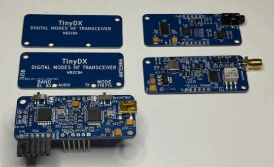
TinyDX consists of these boards.
I chose to use 0603 parts for SMD caps and resistors to keep things as small as possible. Of course this creates a challenge. It is hard to hand solder 0603 parts so I send my fabrication files to www.jlcpcb.com for them to fabricate and pick and place these boards for me in a professional setup.
I am adding a guide how to order smd populated boards from JLCPCB in my TinyDX github site located in this link:
https://github.com/WB2CBA/TinyDX—Tiny-Digital-Modes-HF-Transceiver
All files needed for this fabrication process is in github folder:
There are three SMD populated boards and one top/bottom cover board.
For that cover board we have a gerber file and that’s it.
For all SMD boards we need 3 different files to be sent to JLCPCB as in that guide of ordering I explained this. These files are for example for Main Board:
- GERBER TINY_LT_MAIN.ZIP – This is the gerber pcb file and should be uploaded as a zip file. Do not extract and upload!
- BOM_TINY M.csv – This is Bill Of Material File which contains all parts of that specific board, footprints of each SMD part and a JLCPCB part code starting with C . With this file JLCPCB knows which part I chose from their part library that will be placed for that specific board. This BOM is specific for JLCPCB and those parts are from JLCPCB part library.
Here is the link for JLCPCB Parts library:
https://jlcpcb.com/parts/componentSearch
To see which part is used and all data specs for that part just substitute C part number from BOM to search area of JLCPCB parts library and all details of that specific part will be displayed.
- TINY M-top-pos.csv – This file is called the footprint position file or commonly known as CPL file. This file tells the pick and place machine which part to pick and how to orient the part in relation to the pcb and where to place. This file is arranged specifically for JLCPCB pick and place rules. It won’t necessarily will work with another pcb manufacturer.
That’s all for hardware side of things.
Now how we to put all together to have a working Transceiver.
First, we need to solder couple of things that are through hole and not included in SMD manufacturing.
These are:
- On Main Board, FTDI connector should be soldered first. I generally don’t solder header to ISP connector as it increases overall height. Instead, I use 2×3 pin male header and forcefully hold it in place of ISP at an angle to get a good electrical connection while programming bootloader. This bootloader programming step is done once; we won’t need ISP again so no need to solder in place.
- On TX Board, Transformer T2-613-1 KK81+ needs to be soldered by hand. Also, SMA Antenna connector.
We start with Main board and two 6 pin male 20 mm headers. Solder those in as in the above photo.
Then we prepare these 6mm headers and M3 screws and nuts.
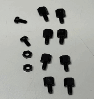
Altogether we need:
8 x 6mm plastic female to male M3 spacers
2 x M3 plastic bolts
2 x M3 plastic nuts
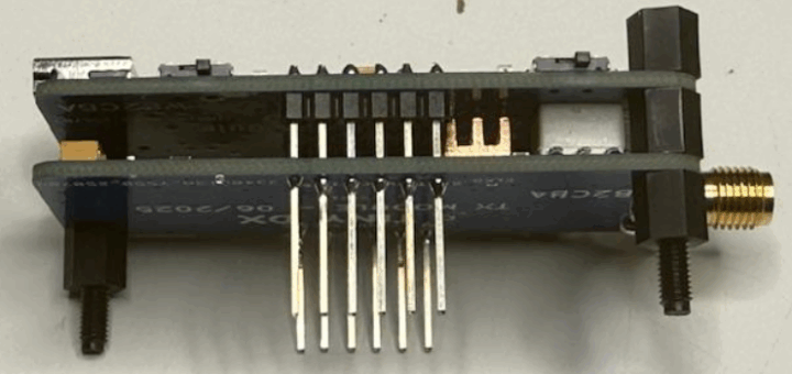
We stack TX board under the main board and screw in with 6mm spacers as in the photo and solder 6 pin headers to TX board. I also added a tiny heatsink for 74ACT244 just in case. The Efficiency of this RF Power amplifier is around 75% and a heatsink is not a must but it won’t hurt either to add one.
Next we stack in RX board and bolt in another set of 6mm spacer. Solder 6 pin headers.
We screw top and bottom plates which are identical. For bottom plate we rotate a top plate 180 degrees on longer axis and screw in. This completes building TinyDX hardware.
- Programming TinyDX:
TinyDX uses an ATMEGA328P/AU Micro-Controller.
First step in programming this controller is to upload Arduino Uno bootloader.
TinyDX firmware is programmed in Arduino C language. We will use Arduino IDE to upload TinyDX Firmware emulating Arduino Uno. That’s why we need Arduino uno bootloader in Atmega328P/AU.
Here is an article describing in detail how to use an Arduino to program bootloader:
https://docs.arduino.cc/built-in-examples/arduino-isp/ArduinoISP/
This YouTube video covers in detail how to upload Arduino Uno bootloader using another Arduino uno as programmer and ISP header which will work for our purpose:
https://www.youtube.com/watch?v=ToMrxnRNHM4
TinyDX ISP Pinout:
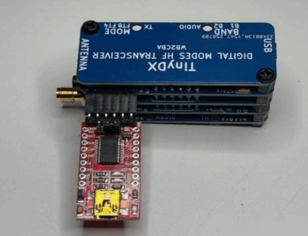
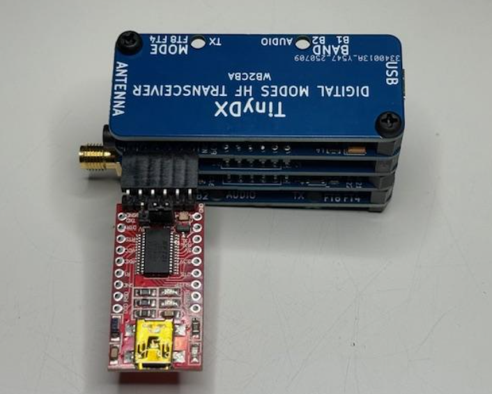
After uploading Arduino uno bootloader now we need to plug in USB to Serial adapter to TinyDX as shown below and upload TinyDX firmware.
TinyDX Arduino firmware is in this link:
After connecting TinyDX to PC via USB to TTL adapter open TinyDX firmware in Arduino IDE and select board as Arduino Uno and upload firmware like uploading to any other Arduino Uno board.
On First power up Red TX Led blink 3 times indicating TinyDX is booting and ready.
USB to TTL adapter can be FTDI pin layout any 5V adapter like this one:
How to operate with TinyDX:
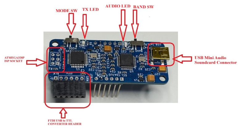
Above photo shows all connections and switches of TinyDX.
- Band Switch. This switch can select between two bands. The default bands on TinyDX firmware are B1 = 20m/14 Mhz band and B2=15m/21 Mhz band.
- Mode Switch – This switch alternates between FT8 mode and FT4 mode.
- Audio LED – This Blue LED is lit when USB is connected and recognized by TinyDX. It flashes when soundcard is recognized and active by the application software such as WSJT/X or IFTX or FT8TW.
- TX Led – A red led lights up when TX is in progress and turns off when RX is in progress.
Operating TinyDX is pretty straightforward.
- Connect USB mini connector to PC or any IOS or Android application. Connect Antenna to your choice of antenna.
- TinyDX does not have CAT Control so no auto frequency or mode changes available.
- When Band or Mode is changed in one of the host digital modes display apps such as WSJT/X the same band/Mode changes must be applied to TinyDX manually to operate on correct band and mode.
- Operating with WSJT/X: In order to operate with WSJT/X from File/Settings/audio/ audio card should be selected. The TinyDX audio card shows as USB Audio Device.
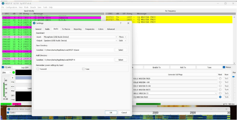
From File/Settings/radio – Rig should be none and PTT type should be VOX.
Set speaker volume to MAXIMUM
- Operating TinyDX with IOS device:
- Install IFTX app.
https://apps.apple.com/us/app/iftx/id6446093115
IFTX is an manual control app. There is no CAT Control. Follow Settings on IFTX manual to set IFTX. First enter callsign and Maiden Grid Locator. IFTX also has an auto locator switch. When On the current locations maiden grid will be transmitted. Don’t forget to match IFTX band and mode settings with TinyDX band and mode settings.
Operating on an Android Device:
To operate on any Android device, we have to app choices, FT8CN or FT8TW.
I will strongly suggest FT8TW as an app. FT8TW can now work in FT8 and FT4 modes.
FT8TW can operate with CAT mode though we can’t use it with TinyDX so again on settings disable Rig as none. FT8TW should automatically recognize TinyDX sound card.
Does TinyDX work:
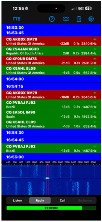
IFTX SCREENSHOTS of QSO on IPHONE 16 Pro Max
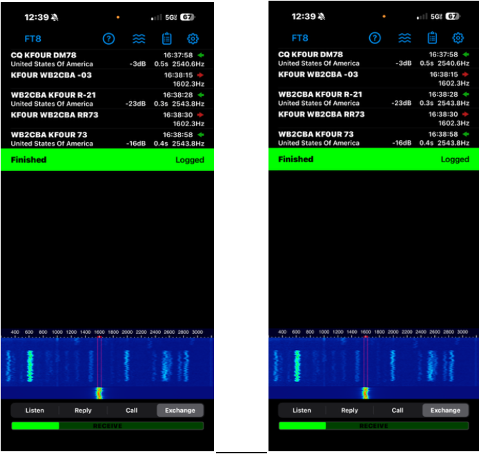
IFTX RX SCREEN
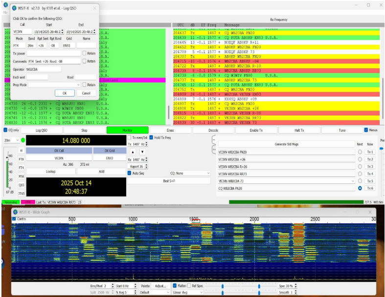
Working on WSJT/X
Final Thoughts
TinyDX is a demonstration of what’s possible when modern Amateur Digital Communication Modes meet compact design. By combining modular PCBs, efficient RF circuitry, and USB power compatibility, it brings real-world practicality to the world of highly portable QRPp operations. Whether built for experimentation or lightweight field communication, TinyDX stands as an example in minimalist ham radio design.
Here is a short Youtube video of TinyDX in action:
https://www.youtube.com/watch?v=lumVageEz0A
Barb WB2CBA – 10/2025