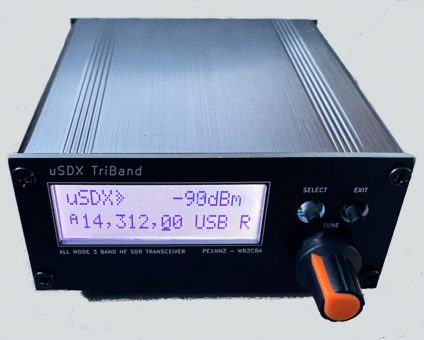
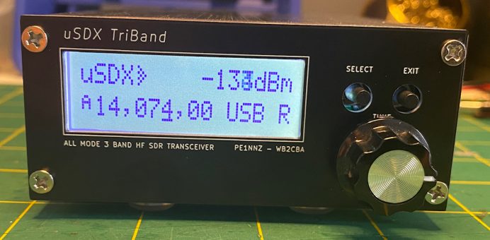
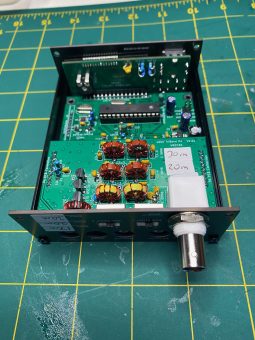
uSDX TriBand SDR All Mode QRP Transceiver
UPDATE!
Please follow this link for 8 Band Version RIG
Please follow this link for Quad Band Version RIG
uSDX TriBand – 3 band SDR All Mode QRP Transceiver
I started my uSDX adventure in March 2020 with modifying a QCX transceiver for SDR SSB using PE1NNZ Guido’s Arduino firmware and modification recipe.
Here is Guido’s github web page where all started from:
https://github.com/threeme3/QCX-SSB
After modifying my QCX kit to SSB I embarked on a quest for the smallest and capable DIY SOTA portable transceiver. In this quest I designed two pcb for Guido’s Arduino firmware. Here are the links for those:
https://antrak.org.tr/blog/usdx-a-compact-sota-ssb-sdr-transceiver-with-arduino/
https://antrak.org.tr/blog/projeler/usdx-an-arduino-based-sdr-all-mode-hf-transceiver-pcb-iteration-v1-02/
And here are the links for related peripherals I added to make these transceiver designs portable, efficient and multiband:
https://antrak.org.tr/blog/usdx-sdr-ssb-sota-transceiver-battery-pack/
https://antrak.org.tr/blog/projeler/linear-rf-power-amplifier-for-usdx/
https://antrak.org.tr/blog/usdx-multiband-low-pass-filter/
uSDX Triband highlights and why another uSDX Transceiver pcb design:
uSDX PCB V1.02 and it’s peripherals like battery pack and multiband serial resonance filter was pretty compact and efficient to serve the backpacking SOTA qso adventure. But… there was always a but in my head. Below I will try to explain the differences and short comings of V1.02 pcb and why I started a new pcb design with a completely new form factor.
Short comings of V1.02 pcb:
– Didn’t have a protective case and this bothered me a lot. Although it was protected with face plates on top and bottom, the sides were open to any condition.
– It was multiband with the add-on multiband adapter but everything was hanging and vulnerable to damage if not protected in a protective case in my backpack.
– With all the add-ons it was still hefty!
– Performance wise it was pretty good with close to 5 watts output and served me well on majority of my digital qso on FT8 and FT4.
What bothered me most was the rather awkward flat controls and outputs all around the rig design. It didn’t feel like a classic YAESU FT817 or any other similar radio where the inputs outputs and the antenna is at the back of the rig and controls in the front with display and protected with an aluminum durable enclosure.
So what does uSDX TriBand design brings to the table:
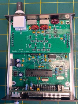
– An Aluminum enclosure! Which protects all the electronics as it should be. So you can easily toss it into your backpack and you don’t have to worry about damage.
– Small enough to fit even in your jacket pocket and easy to travel with. It is 100 mm x 88 mm x 38 mm(3.9” x 3.5” x 1.5”)
– It is 3 band with separate PA board which means multiple PA boards can be switched to add multiples of 3 bands choices.
– Looks more like a classical pro TRX look with pcb front and back face plates to be bolted on aluminum enclosure.
– It has an ISP connector for ease of firmware upload.
– It has SDR I/Q output pin header on PCB which can be extended with a 3.5 mm jack cord to connect a PC soundcard audio line input to decode with various SDR software as any SDR dongle.
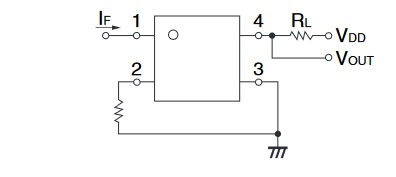
– It has a PTT OUT jack driven with a Solid State opto coupled relay capable of driving 500 mA relays for example an external RF Power Amplifier relay directly.
Apart from these my design philosophy didn’t change a bit which is KISS (Keep It Simple Stupid), easy to build just with a fine tip soldering iron and easy and simple to operate in the field:
– Schematic of uSDX is same as PCB V1.02 hence the 3 band lpfs and band switches.
– It is mostly through hole components. all IC’s are smd due to less real estate area on pcb but can be soldered easily with a fine tip soldering iron. If FST3253 can be soldered in V1.02 with a soldering iron then these ICs all have same pin pitch.
– It has the option of both Si5351 smd or SI5351 Module option. With the SI5351 module this rig can be soldered only with a fine tip soldering iron.
– Band switching has the same topology as my V1.02 pcb multiband module using two slide switches to switch between bands. uSDX firmware supports relay controlled automatic band switching but I avoided it on purpose to save space and for the sake of simplicity in configuration of choosing just 3 bands without all those relays etc.
– LPF design on uSDX TriBand is Manuel Klaerig, DL2MAN’s efficient serial resonance filter which can efficiently deliver 3.5 to 5 watts depending on band. Thank you Manuel for this great lpf design.
– uSDX Triband uses a COG (Chip On Glass) 2×16 LCD from New Haven Display which is relatively cheap, small and thin to keep the unit compact. I also designed a Standard 2×16 LCD display pcb as a classic display option. The only drawback of that approach is suggested aluminum enclosure is not an option anymore, it won’t fit.
As a summary uSDX Triband is an upgraded version of uSDX V1.02 pcb with a smaller display, multiband capability built in and stacked in an aluminum enclosure with bonus features on top of V1.02 PCB.
Sourcing Parts that are different than V1.02 PCB:
uSDX Triband uses most of the parts of V1.02 PCB design BOM. Here I will outline the parts that are specific to uSDX Triband and where to procure them.
Aluminum Enclosure:
I used this aluminum enclosure from Amazon but I think Ebay holds a similar enclosure too. I designed the pcb specifically for this enclosure to slide in where the enclosure has pcb rails which holds the pcb in place.
Here is the link for aluminum enclosure:
New Haven COG LCD Backlight 2×16 Character LCD Display:
I got my displays from Digikey but Mouser also holds these displays. Here are the links for both:
Digikey:
https://www.digikey.com/en/products/detail/newhaven-display-intl/NHD-C0216AZ-FSW-GBW/2165869
Mouser:
Band Slide Switches:
Digikey:
https://www.digikey.com/en/products/detail/e-switch/EG2315/101778
SMD IC’s:
3253:
For this you can use SN74CBT3253CD from Texas Instruments as FST3253 is not easy to find anymore. Here is the link from DIGIKEY:
https://www.digikey.com/en/products/detail/texas-instruments/SN74CBT3253CD/1569721
74ACT00:
https://www.digikey.com/en/products/detail/texas-instruments/SN74ACT00DR/556027
LM4562MAX:
https://www.digikey.com/en/products/detail/texas-instruments/LM4562MAX-NOPB/3738987
SI5351 SMD:
Digikey:
https://www.digikey.com/en/products/detail/silicon-labs/SI5351A-B-GTR/6575757
LM1117 – 5.0 Regulator:
https://www.digikey.com/en/products/detail/texas-instruments/LM1117MP-5.0-NOPB/363589
IRLML 2060 Mosfet:
I included the option to use a PA pcb with IRLML 2060 Mosfets. If you decide to build your PA with these here is the Digikey link:
https://www.digikey.com/en/products/detail/infineon-technologies/IRLML2060TRPBF/2271917
Rotary Encoder:
I used a short shaft bourns rotary encoder with 24 pulse option and no detents which gives a much smoother tuning without those annoying clicks. Here is the link from Digikey:
https://www.digikey.com/en/products/detail/bourns-inc/PEC11R-4015F-S0024/4499668
Solid State Relay For PTT OUT:
Tactile Switches:
Tactile switches can be any of the tactile pushbutton through hole switch with a lever shaft length not less than 6 mm. Actually 6 mm lever shaft size fits perfect.
Here is a link from Digikey for such a tactile switch with 6 mm protruding shaft:
https://www.digikey.com/en/products/detail/schurter-inc/1301.9306/7602715
Rest of the components are similar to V1.02 PCB components, all through hole.
Let’s dive into building uSDX Triband!
I would strongly recommend to read these two articles about V1.01 and V1.02 pcb before diving into building uSDX TriBand as these have tips on building and testing uSDX that will help.
https://antrak.org.tr/blog/usdx-a-compact-sota-ssb-sdr-transceiver-with-arduino/
https://antrak.org.tr/blog/projeler/usdx-an-arduino-based-sdr-all-mode-hf-transceiver-pcb-iteration-v1-02/
uSDX TriBand consists of 3 separate PCBs that come together to complete the transceiver as a unit. I will try to iterate these in three different sections for ease of explaining.
I didn’t add schematics into this article not to make it longer than it is. All the schematics are in the zip file at the end of this article.
Let’s start with the LCD pcb:
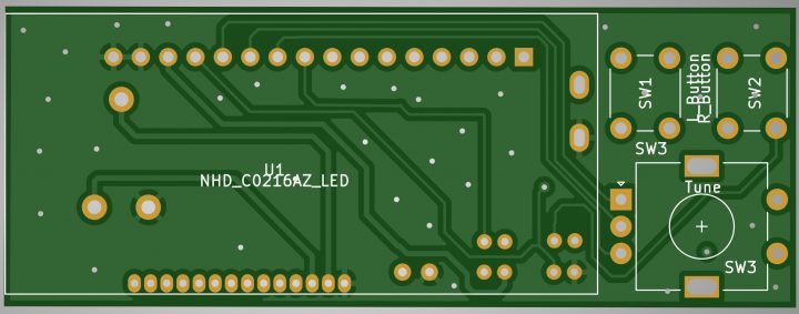
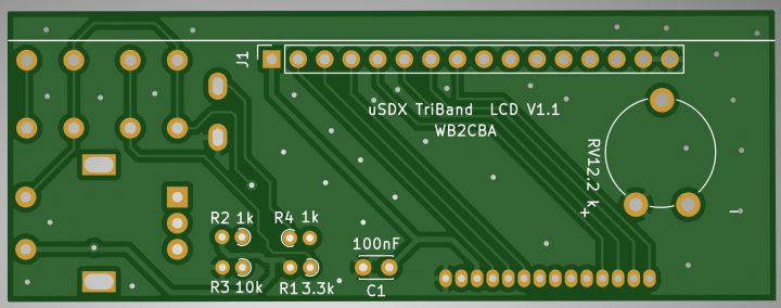
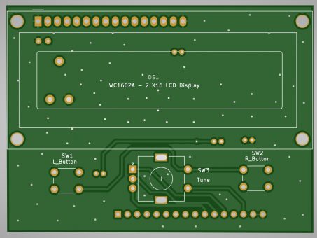
These are pcb layouts of LCD pcb which also holds the rotary encoder and two tactile switches for tuning and menu control.
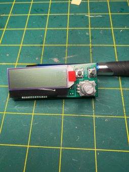
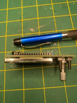
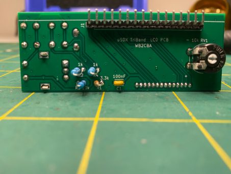
These are photos of completed LCD PCB. As can be seen from photos components needs to be soldered at the back of the LCD pcb and display with rotary encoder and pushbutton switches are on the display side.
There is also a 90 degree 16 pin male header that will be the connection between LCD pcb and Main PCB.
Here is a safe check list how to build LCD pcb.
1- Solder R1, R2, R3 and R4 with C1 and RV1 on component side as in the above photo.
2- Solder 90 degree male header as in the photo. The side view photo gives a clue how to orient and solder 90 degree header correctly.
3- Cut the excess header pins and pot RV1 pins from display side as flush as possible so that they won’t interfere with LCD and push it excessively out when we solder LCD.
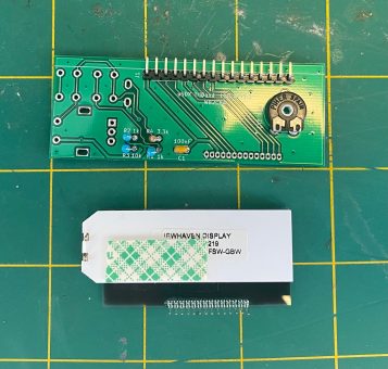
4 – cut a strip of double sided tape and place it as in the above photo. This will fix and raise the LCD from below solder pads of header and pot RV1. There is a gap under the LCD where the passive components are aligned with so there isn’t any interference problem there. Now align the LCD with white LCD border lines and push it into it’s place with double sided tape glues onto pcb so that it will stick and fix the LCD securely on PCB. Check if the LCD is aligned with white lcd border lines and as parallel as it can be with pcb edge. Adjust if necessary. Now we are ready to solder it. Solder two side LED backlight pins and LCD pins thoroughly.
This completes LCD soldering. Put it aside and let’s dive into Main PCB.
Main PCB Soldering Tips:
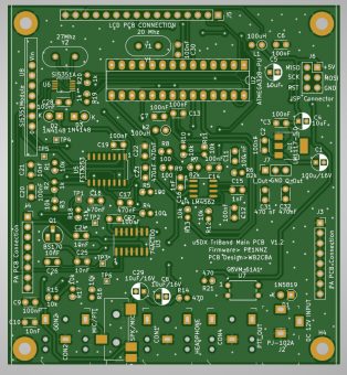
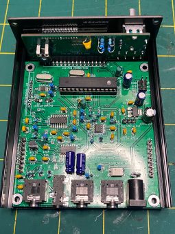
Main PCB holds majority of the components of uSDX Transceiver except the RF Power amplifier section and LCD display section.
Before starting to solder any component we have to make a decision on SI5351 signal generator:
– If we choose to solder the SMD version of SI5351 then this is the first part to be soldered and this is not for faint hearts. The method I use is Hotair rework soldering with flux and liquid solder. Though it needs a hotair rework station. Hotair rework stations are relatively cheap nowadays and it is a great tool to have. There are other methods like flooding with solder and removing the excess with a solder wick etc. Youtube has a lot of videos for smd soldering techniques.
– The second method is to use one of those SI5351 Modules which can be grabbed from Adafruit, Amazon, Ebay, Aliexpress etc.
Here is a link for such a module:
https://www.adafruit.com/product/2045?gclid=CjwKCAiA25v_BRBNEiwAZb4-Zc8mkQ8HB9uvSq8C1FeR0jjXmsh3FFNFEoPE0a6N3RU5pOv9HsT7aRoCmlcQAvD_BwE
If this route is preferred then this module needs to be modified as we did in V1.01 and V1.02 pcb. I included this modification in this article in the link:
https://antrak.org.tr/blog/usdx-a-compact-sota-ssb-sdr-transceiver-with-arduino/
If SI5351 module will be used then we don’t need to install SI5351 smd anymore and related parts like 27 mhz XTAL, two 1N4148 diodes and R19,20 1k resistors and C28 100nF cap.
Solder SI5351 Module as the last part to go on the main pcb. If it is soldered before all the other parts in then when we tip over the pcb for soldering it will lift awkwardly one side of the pcb which will make soldering harder.
Now SI5351 dilemma is out of the way here is the route I follow when installing and soldering parts. This is my preferred method as a suggestion. Everyone has their own preference.
– All SMD parts are soldered first. These are 3253, 74ACT00, LM4562MAX, LM1117-5.0 V, smd SPK/MIC jack.
This is important as it will be hard to reach these when we first populate around them.
– Then I install all the peripherals like MIC/PTT, Headphone, PTT OUT and DC Barrel Connector jack, 28 pin DIP socket for Atmega 328, PA male headers, SDR I/Q header, SPI header.
– Then comes BS170, SSR relay G3VM-61A1, 1N5819 diode and crystals.
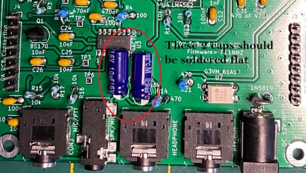
– Now this is the turn of capacitors. I start with C8 and C29 10uF/16V caps first. Here we need to mount two of the 10uF capacitors flat on their belly as these can interfere with PA pcb that is going to sit on top of them if they are soldered vertical. These capacitors are C8 and C29.
– By the way the letter K means Cathode of a diode which is the ring side!
– Then I solder remaining resistors after capacitors.
If you chose SI5351 Module route then now it is a good time to solder SI5351 Module in it’s place. Make sure that you solder the module directly onto the pcb without any female header using 90 degree male headers. If female header is used on main pcb side with male header on SI5351 Module then it will raise the module and might not fit when the aluminum enclosure is closed.
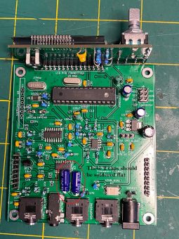
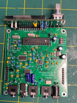
Now it is time to mate Main PCB with LCD PCB. Insert LCD PCB header to it’s holes as in the photo below:
Make sure that LCD is perfectly aligned 90 degrees to Main PCB then solder one of the pins of male header and check the 90 degree alignment. If you are satisfied with the alignment then solder all pin header to main pcb. Do not use female and male headers with the thought that lcd pcb can be removable. It won’t fit into this aluminum enclosure! Space is really tight inside!
Now it is a good time to check if the main board + LCD board combination is working as expected. First check all the components and solder joints for any defects, cold joints and make sure all parts are correctly installed in their respective holes.
Program your atmega328p with one of the methods out there of your choice with Firmware version V1.02J which is included in the zip file at the bottom of this article.
If you used smd SI5351 and 27 mhz crystal then your firmware is uSDX V1.02J_27mhz.
For SI5351 Module please use uSDX V1.02J_25mhz one.
You can use my Arduino uno board swap method if you like which I explained in this article:
https://antrak.org.tr/blog/usdx-a-compact-sota-ssb-sdr-transceiver-with-arduino/
Plug your programmed Atmega328p in it’s socket.
Now you need an adjustable power supply which will be adjusted to 12V and if there is current limit then limit the current to 100 milliamps. If your power supply can measure current when you power up you should see a current draw of around 60 milliamps. If you don’t see any activity on LCD then trim the pot towards “+” mark on the pcb all the way to the end.
If you see backlight and characters on LCD display then you have an alive main board LCD combination. Play with the rotary encoder and push buttons to see all is working fine.
Soldering Power Amplifier PCB:
Now we can start soldering our Power Amplifier pcb.
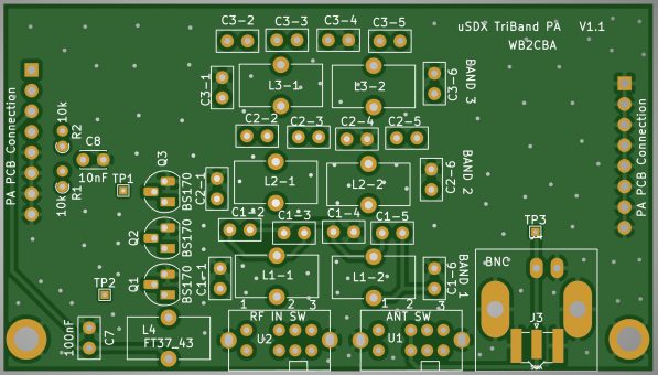
This is PA PCB:
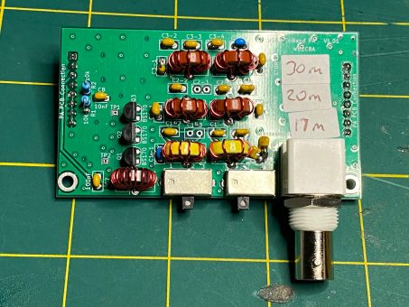
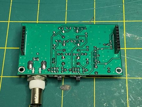
This is how the completed PA PCB looks like:
Component Side:
Solder side of PA PCB.
I generally start with 3 x BS170s then install all the caps and resistors then BNC Connector. The female headers are soldered on solder side. And the band switches.
Now we have only Toroids left out. Depending on your band choice wind the toroids accordingly. Also the band capacitors will be chosen to match the required band.
For Toroid and cap values for your bands please use below table:
I strongly recommend to use a BNC Connector, SMA connector won’t align with Back face plate with this aluminum enclosure.
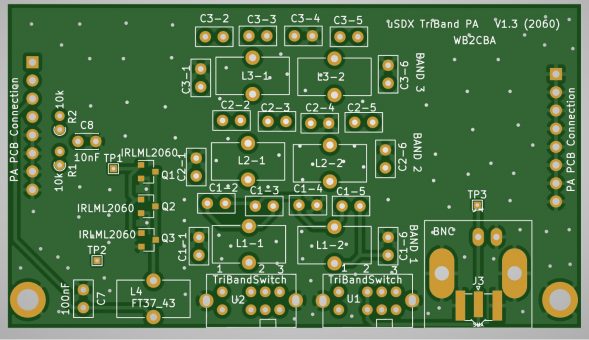
IRLML 2060 PA PCB:
Out of curiosity I also designed a Power amplifier PCB using 3 x IRLML 2060 mosfets. It worked surprisingly well.
Here is the PCB of IRLML 2060 PA:
This is the real deal installed:
I soldered only one band for test purposes on IRLML2060 PA PCB but in reality everything is similar to building BS170 PA. LPF band values can be obtained from above table.
I tried only 20m, 30m and 40m band values for caps and Toroid turns. I didn’t try 60m and 80m values but they are shamelessly stolen from Manuel’s design so I am confident that they will work! :) I am working on 17m,15m and 10m LPFs. When I have working values I will post here as an update.
Now the moment of truth: Testing…
Now all pcbs are built and ready to rock’n’roll and now it’s time to test!
To work through testing smoothly we need instruments! And here are these:
– A multimeter
– A bench power supply with 12V, 1 amps capacity at least.
– A Frequency Counter with hertz resolution up to 30 mhz.
This is a cheap frequency counter for the task in hand:
https://www.aliexpress.com/item/33007930974.html?src=google&albch=shopping&acnt=494-037-6276&isdl=y&slnk=&plac=&mtctp=&albbt=Google_7_shopping&aff_platform=google&aff_short_key=UneMJZVf&&albagn=888888&albcp=9765122064&albag=101238896618&trgt=892975210502&crea=en33007930974&netw=u&device=c&albpg=892975210502&albpd=en33007930974&gclid=CjwKCAiA25v_BRBNEiwAZb4-ZZTSJ93bt7yiaZq1pTUA2iAsfKGzU8e1aZNHPr4rTtWmlV6k35eMWhoCUG8QAvD_BwE&gclsrc=aw.ds
– A RF powermeter capable of measuring up to 10 watts.
– A dummy load up to 10 watts.
With these instruments it’s a breeze to work out adjustment and testing of this rig.
Here is a simple test procedure that I use:
1- Connect your dummy load at PA output.
2- Connect your power supply in series with current measurement mode on your multimeter. Use a second voltmeter if you have for observing voltage. Ofcourse if you have a bench power supply with Voltage and Current displays then ignore these steps. Just connect your PSU to uSDX Triband.
3- Now power up and see how much is current draw on RX. It should be still around 60 miliamps.
4- Let’s say we are on 20m band so tune to USB 14000000 mhz in the lcd screen then enter menu by pressing left button and scroll up to menu item 8.1 Freq which is local oscillator frequency. Connect your frequency counter probe to SI5351 “0” output and ground connection. Now click rotary encoder once then rotate the encoder such that you see 14000000 mhz on your frequency counter. The tick is to match displayed frequency to SI5351 output frequency. If you see 14000000 Mhz then your display screen matches your local oscillator frequency by hertz. Now click left button once more to store and then click right button to exit from menu. You are done!
5- Now we will adjust RF power output. Select from band select switches the desired band. Don’t forget both band switches must be in the same position meaning that if band position 1 LPF is the band you wanna work on then band select switch 1 and 2 must be both in 1 position. And these have to match the display tuning band
Plug in your microphone to MIC/PTT input and connect your rf power meter. Select CW mode with pressing right pushbutton.
Press left button and enter the menu area and scroll until 8.3 PA Bias MAX and lower that to 100. Then scroll to 8.2 PA Bias Min and scroll until 20.
Now press PTT and check your power output. If all is good then you should see something around 3.00 to 3.50 watts rf power output. Now record your power output with your current drawn at this output.
Now enter menu 8.3 PA Bias max and increase from 100 in increments of 10 and transmit in each increment to see your rf output and current. If you are in a state that current is increasing but rf power is staying at where it is without significant increase then we are saturating the PA mosfets into inefficient zone so we need to roll back until rf power stays same but current decreases. When we see rf power also roll back then we are set, leave it like that.
Now uSDX TriBand is ready for a qso!
– For IRLML 2060 PA start with PA Bias Max = 40 as these mosfet require lower bias value.
Installing uSDX TriBand into it’s aluminum enclosure:
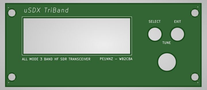
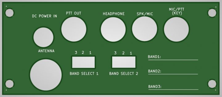
These are two pcbs which will be bolted to front and back of the enclosure:
These are shown green here due to gerber viewer display selection although when I ordered mine I ordered in black mask color to match Aluminum enclosure color which is black. Tastes can differ so feel free to choose which color you like.
Now first thing we should do is to install front face plate with top two bolts into one half of enclosure. Then slide in uSDX pcb in it’s rail. The whole contraption should be up side down which is how it should be installed. See photo:
Now install the back face plate and bolt on:
Don’t forget to mark your bands on the PA pcb as in the photo. This will be very handy when troubleshooting.
Now Mark the respective bands also at the back plate as in the photo to guide you which band is which when changing bands.
Now mate the other half of the aluminum enclosure and bolt on then you are done.
Don’t forget to install rotary encoder washer and screw. Also same goes for BNC connector washer and screw.
Some helpful tips on usage of connectors:
Headphone Jack:
Headphone connector is 3.5 mm standard TRS jack.
Tip – Audio out
Ring – Audio out
Sleeve– GND
This jack audio output is lowered with a 470 ohm resistor to suit feeding straight into PC mic input, earphones etc.
MIC/PTT(KEY) Jack:
This jack is also 3.5 mm standard audio jack in TRS combination.
Tip – Mic input
Ring – PTT
Sleeve – GND
In CW KEY INPUT MODE:
Tip- DAH
Ring- DIT
Sleeve – GND
SPK/MIC Jack:
This is a 4 pole jack configured as TRRS.
This is used to connect a hand Speaker/Microphone combination and uses BAOFENG UV-3R handheld cheap speaker/microphone similar to this one:
https://www.ebay.com/i/401863211871?chn=ps&norover=1&mkevt=1&mkrid=711-117182-37290-0&mkcid=2&itemid=401863211871&targetid=1068323860270&device=c&mktype=pla&googleloc=9003562&poi=&campaignid=10459841961&mkgroupid=104612009980&rlsatarget=pla-1068323860270&abcId=2146002&merchantid=6296724&gclid=CjwKCAiA25v_BRBNEiwAZb4-ZRvy1rwtRGU3fC6uOA1VcBckiyfsw1ZDwmYpcbaxb-eFdBSkii7VZRoCYVgQAvD_BwE
Connection points are as follows:
TIP :SPEAKER
RING 1:MIC
RING 2:PTT
SLEEVE: Gnd
PTT OUT Jack:
This jack uses 3.5 mm standard audio jack.
TIP :OUT pin of SSR to external device
RING: OUT pin of SSR to external device
SLEEVE: GND
This might give an idea how a relay should be connected to output of SSR. Basically it will be inserted between Tip or ring and VCC of external device to switch on and off. This might be a relay of a Power amplifier. Also sleeve of jack should be connected to gnd of external device.
This PTT OUT function can be used only with version m firmware which will be released soon as it is controlled by firmware and delays can be introduced between activating SSR and actual transmission from menu screen. It turns on when PTT is activated.
SDR I/Q output header:
Pablo Cardenosa, EA2EHC gave an invaluable idea of using I and Q outputs from uSDX to feed into a PC soundcard mic input and using a PC SDR software like HDSDR to receive and waterfall functions.
For this I used HDSDR. Here is the link:
http://www.hdsdr.de/
I put together a short youtube video demonstrating this SDR I/Q output:
2×16 Standard LCD PCB:
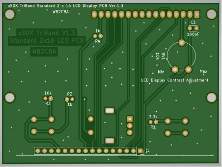
I also designed a LCD 2×16 character PCB as used in V1.01 and V1.02 pcb designs. This is for fellow hams who prefer to take a route with a bigger display than Newhaven COG display then this creates a nice alternative. I must add that I designed this LCD PCB but didn’t build and test one so if anyone decides to take that route beware that you are on your own and please let me know if it works so that I can update this article and let me know if there is a problem I can correct and update!
Here is the layout of 2X16 Standard LCD PCB:
LCD Side Layout
Component Side Layout:
128×64 OLED Display Option:
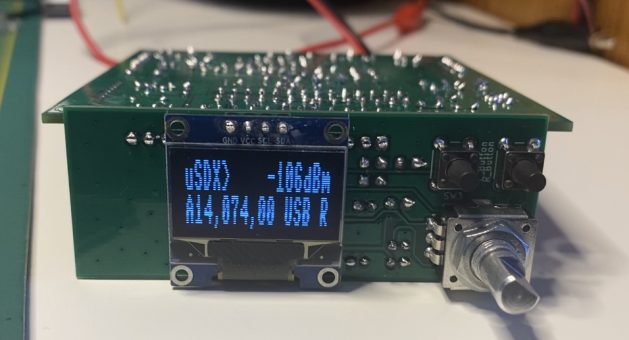
uSDX TriBand can be build with 128×64 OLED option if LCD is not the desired display choice.
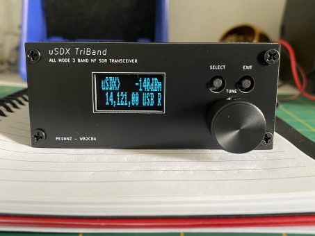
Here is uSDX TriBand with OLED Display:
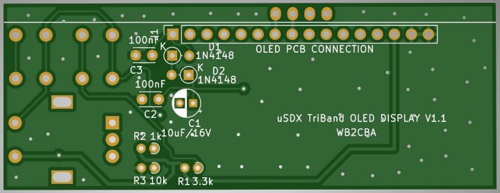
Soldering and building OLED Display for uSDX is similar to COG LCD display. Start with components and 90 degrees header soldering and attach a tiny double sided tape to hold OLED display in place also raising it couple of millimeters.
There are two important points we need to pay attention:
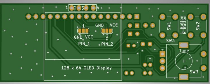
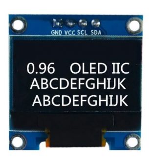
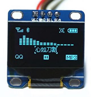
1- Choosing jumpers for VCC and GND supply pins OLED Display. This is important as 128×64 OLED displays come in two different VCC and GND pin orientation. As in the photos below:
Top OLED has Gnd as pin 1 and VC as Pin 2 and the bottom OLED has VCC as Pin 1 and GND as Pin 2.
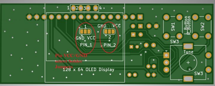
To choose the correct pin combination to suit the OLED display chosen I added two solder jumpers:
These Jumpers correspond to Pin1 and 2, VCC or GND position. For example if we selected an OLED Display with pin 1 = VCC and Pin 2 = GND then Pin 1 jumper should have a solder blob between VCC and 1 and Pin2 jumper should have solder blob between GND and 2. Now we are set as pin 1 VCC and Pin 2 GND. Same applies to GND/VCC version of oled display opposite of what we did on soldering jumpers.
One more important thing is to solder these jumpers before we install the OLED display in place.
2- Soldering and cutting OLED Display Pins:
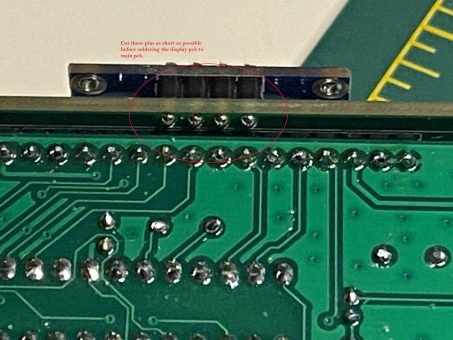
First the 16 pin 90 degrees male header needs to be soldered in place. Then cut the OLED pins around 2 to 2.5 mm and then solder the OLED in place. This way OLED pins will be barely stick out and won’t short 16 pin header.
Here are some more photos of Main pcb/OLED pcb interaction:
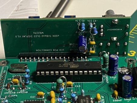
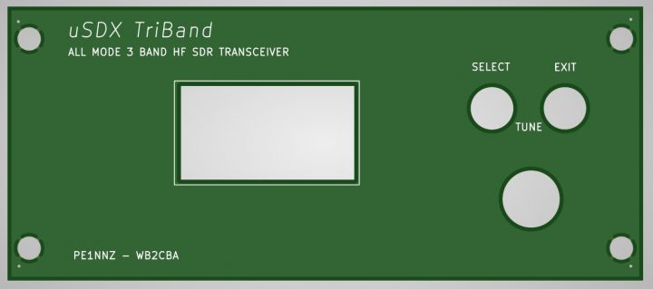
OLED Display required a new front face plate:
OLED version works only with OLED firmware which I have added in the firmware section of uSDX TriBand zip file. LCD ones won’t work with OLED display.
I am including a zip file with all the necessary files to build this rig at the end of this article:
The zip file is named as : uSDX TriBand_Revised_06_18_2021.zip
It includes:
– GERBER Files of all pcbs
– Schematics of all pcbs
– Pcb layouts of all pcbs
– uSDX firmware for 25 mhz and 27mhz SI5351 options optimized for uSDX TRiBand.
So this is uSDX TriBand which is my take on a through hole, simple to build and operate 4 to 5 watts pocketable multiband QRP SOTA All mode SDR transceiver designed with KISS(Keep It Simple Stupid) philosophy which is my motto in my hobby. A notch simpler than ICOM IC-705!
It was really fun to work on uSDX TriBand project. I hope ham community will embrace, build and use this version of uSDX which will certainly put a huge smile on my face.
If you build uSDX TRiBand please do not hesitate to contact me to share your experience, good or bad which will make me happy to hear from you.
I would like to thank my friend Ken Delap, KX9U for working with me on this project and his endless testing and support.
I also thank Guido, PE1NNZ for his great coding mind and creating uSDX project and software. Without his firmware we will have a nice looking junk!
Thanks to Pablo Cardenosa, EA2EHC for his suggestion and guidance on SDR I/Q output of uSDX to use it as an SDR receiver.
Happy New Year!
Barb WB2CBA
NY 12/28/2020
wb2cba@gmail.com
– uSDX TriBand PCB Project Files are in uSDX TriBand.zip
uSDX TriBand PCB design is released as OPEN SOURCE – FREE For Ham Radio Community to USE without any prohibitions or restrictions.
WB2CBA – Barbaros Asuroglu
Update:
If you are looking for an alternative case for uSDX TriBand here is a solution. Thanks to Scott Baker, KJ7NLA you can make your own 3D Print case. Here is the link of 3D Print case for uSDX TriBand tranceiver.
Update: (19th June 2021)
Another case for 3D Print by Omer Guleray, TB2CPO uSDX Case v1.2 by TB2CPO

